
Dicing tape-integrated film for semiconductor back surface

Inactive Publication Date: 2011-10-20
NITTO DENKO CORP
View PDF2 Cites 7 Cited by
  • Summary
  • Abstract
  • Description
  • Claims
  • Application Information

AI Technical Summary

Benefits of technology

[0015]The present invention has been made in consideration of the foregoing problem and an object thereof is to provide a dicing tape-integrated film for semiconductor back surface which is capable of easily peeling the semiconductor element at the picking-up together with the film for flip chip type semiconductor back surface and thereby capable of improving production yield, and a process for producing a semiconductor device.

Problems solved by technology

As a result, the number of steps increases and production cost and the like increase.
However, in the dicing tape-integrated film for semiconductor back surface described in the above, in the case where close adhesiveness of the pressure-sensitive adhesive layer with the film for flip chip type semiconductor back surface is high, picking-up of the semiconductor element becomes difficult in some cases.

Method used


Image

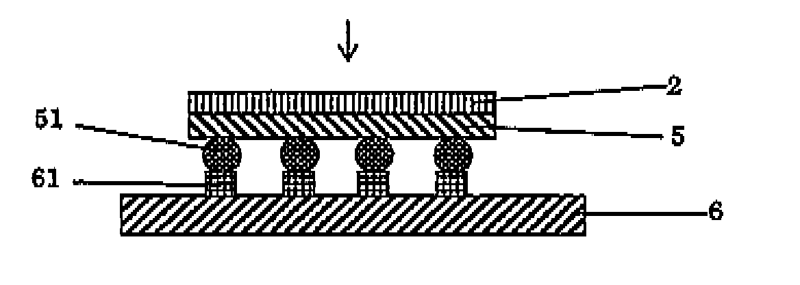
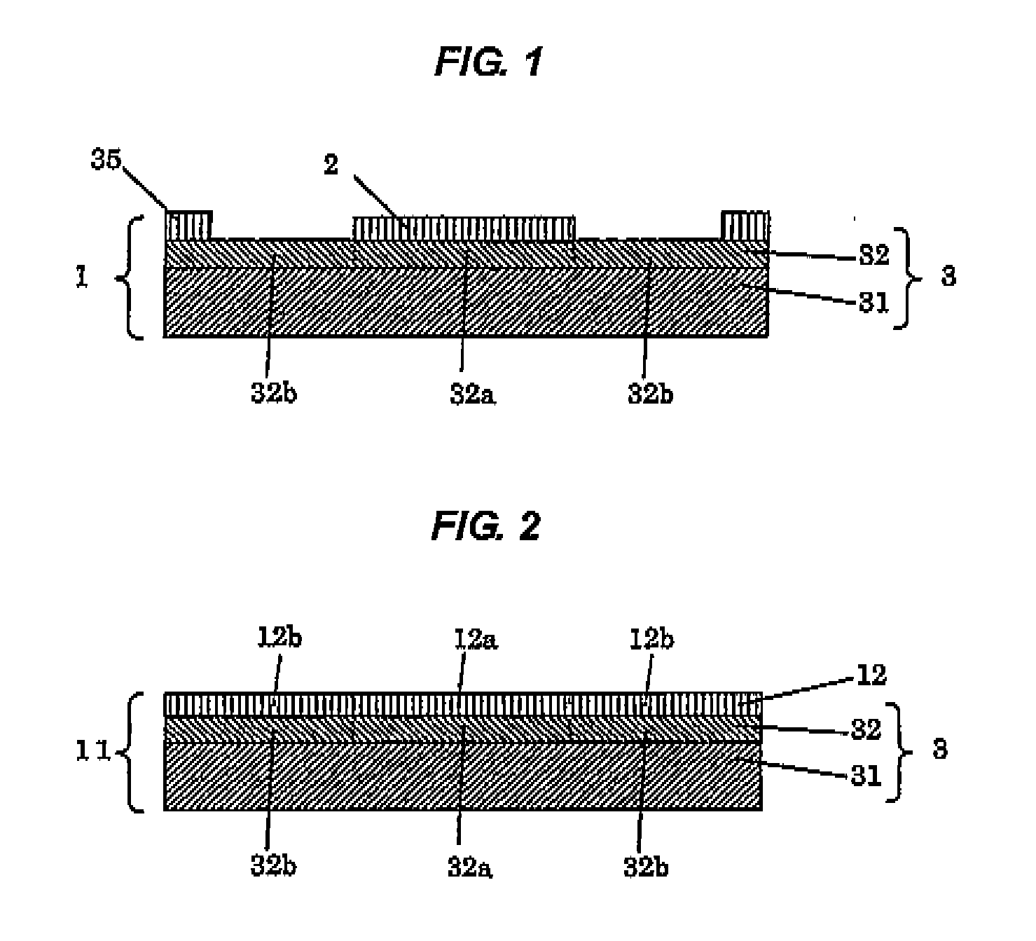
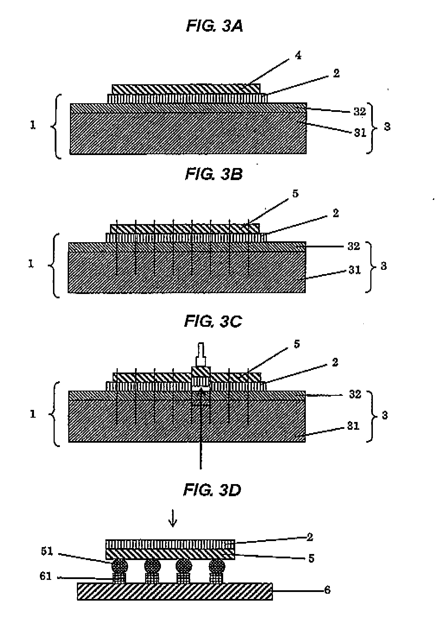
  • Dicing tape-integrated film for semiconductor back surface
  • Dicing tape-integrated film for semiconductor back surface
  • Dicing tape-integrated film for semiconductor back surface

Examples


example 1

Preparation of Film for Flip Chip Type Semiconductor Back Surface

[0169]113 parts of an epoxy resin (a trade name “EPICOAT 1004” manufactured by JER Co., Ltd.), 121 parts of a phenol resin (a trade name “MILER XLC-4L” manufactured by Mitsui Chemicals, Inc.), 246 parts of sphere silica (a trade name “so-25R” manufactured by Admatechs Co., Ltd.), 5 parts of Dye 1 (a trade name “OIL GREEN 502” manufactured by Orient Chemical Industries Co., Ltd.), and 5 parts of Dye 2 (a trade name “OIL BLACK BS” manufactured by Orient Chemical Industries Co., Ltd.) based on 100 parts of an acrylic acid ester-based polymer (a trade name “PARACRON W-197CM” manufactured by Negami Chemical Industrial Co., Ltd.) containing ethyl acrylate and methyl methacrylate as main components were dissolved in methyl ethyl ketone to prepare a solution of a resin composition having a solid concentration of 23.6% by weight.

[0170]The solution of the resin composition was applied onto a releasably treated film, as a release...


PUM

PropertyMeasurementUnit
Sensitivityaaaaaaaaaa

Abstract

The present invention provides a dicing tape-integrated film for semiconductor back surface including: a dicing tape including a base material and a pressure-sensitive adhesive layer on the base material; and a film for flip chip type semiconductor back surface, which is provided on the pressure-sensitive adhesive layer, in which at least a part of the pressure-sensitive adhesive layer has been cured beforehand by irradiation with a radiation ray.

Description

FIELD OF THE INVENTION[0001]The present invention relates to a dicing tape-integrated film for semiconductor back surface having a film for flip chip type semiconductor back surface. The film for flip chip type semiconductor back surface is used for protecting a back surface of a semiconductor element such as a semiconductor chip and enhancing strength. Moreover, the invention relates to a process for producing a semiconductor device using the dicing tape-integrated film for semiconductor back surface and a flip chip-mounted semiconductor device.BACKGROUND OF THE INVENTION[0002]Recently, thinning and miniaturization of a semiconductor device and its package have been increasingly demanded. Therefore, as the semiconductor device and its package, flip chip type semiconductor devices in which a semiconductor element such as a semiconductor chip is mounted (flip chip-connected) on a substrate by means of flip chip bonding have been widely utilized. In such flip chip connection, a semico...

Claims


Application Information

Patent Timeline
IPC IPC(8): H01L23/48B32B7/12H01L21/50C09J7/20
CPCH01L24/81C09J2205/31H01L23/3164Y10T428/2809H01L21/561C09J2201/36H01L2224/81191H01L2224/16225C09J2201/606H01L2224/81007H01L21/6836H01L2221/68327C09J2203/326C09J7/02H01L2924/14C09J7/20C09J2301/208C09J2301/302C09J2301/416H01L2924/00H01L21/78
Inventor TAKAMOTO, NAOHIDESHIGA, GOJIASAI, FUMITERUYAMAMOTO, AKIYOSHITAKAHASHI, TOMOKAZU
Owner NITTO DENKO CORP
Learn More