Integration of microstrip antenna with CMOS transceiver

a microstrip antenna and cmos technology, applied in waveguide devices, resonant antennas, substantially flat resonant elements, etc., can solve the problems of micromachining not being compatible with cmos technology, increasing costs, and raising doubts about mechanical stability, so as to improve mechanical stability, low cost integration, and low interconnection loss

Active Publication Date: 2011-10-27
ADVANCED MICRO DEVICES INC +1
View PDF2 Cites 14 Cited by
  • Summary
  • Abstract
  • Description
  • Claims
  • Application Information

AI Technical Summary

Benefits of technology

[0019]Embodiments of the present invention may thus provide a broad band, efficient antenna for a millimetre-wave wireless transceiver system, giving low cost integration by being compatible with CMOS technology and may also be compatible to other technologies such as SiGe or GaAs, and providing low interconnection losses. Moreover, the use of an under-fill layer with flip chip bonding assists in providing mechanical stability.
[0020]By selecting flip-chip bonding, this invention provides on chip antenna integration bonding which is compatible with standard CMOS technology, and which avoids the significant transition discontinuity losses suffered by wire bonding and wedge bonding at millimetre wave frequencies. Moreover, flip chip mounting enables a low loss connection between the coplanar waveguide formed on the second surface to a microstrip transmission line or other type of connection as may be formed upon a CMOS die upon which the antenna element is flip chip mounted.

Problems solved by technology

However, micromachining is not compatible with standard CMOS technology, increases costs, and may raise doubts as to mechanical stability.
A further significant issue in fabrication of such antennas can be transition discontinuity losses at connections between the antenna and other transceiver elements.

Method used


Image

  • Integration of microstrip antenna with CMOS transceiver
  • Integration of microstrip antenna with CMOS transceiver
  • Integration of microstrip antenna with CMOS transceiver

Examples


Embodiment Construction

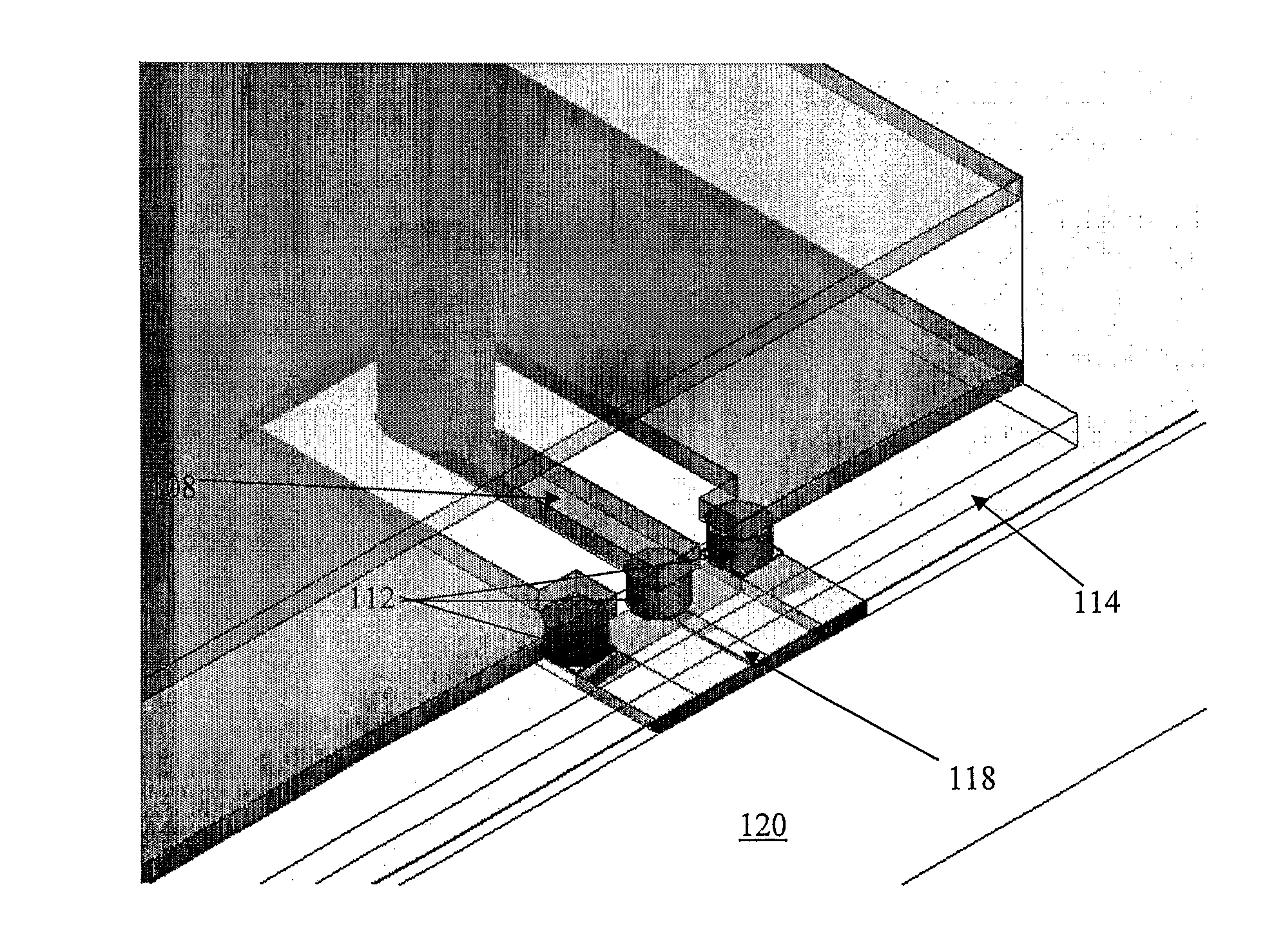
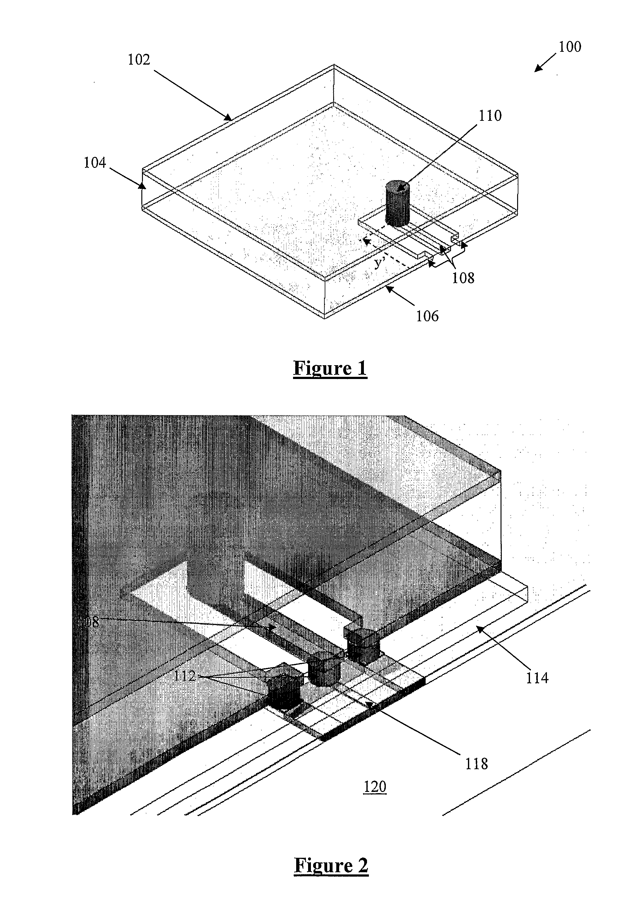
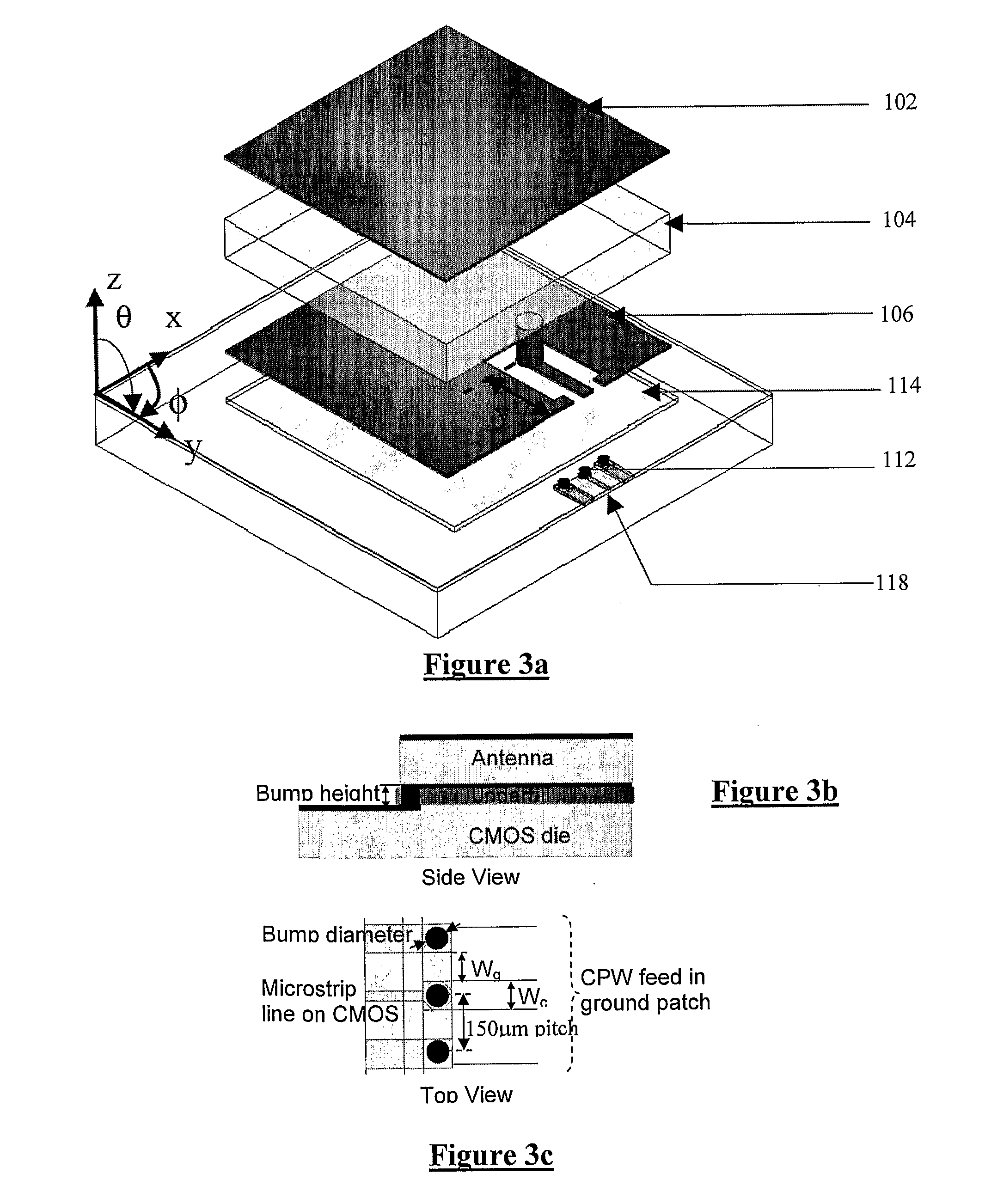
[0036]The basic geometry of a microstrip antenna element 100 in accordance with one embodiment of the invention is shown in FIG. 1. The antenna is comprised of a radiating patch 102 printed on the upper surface of the substrate 104, and a ground plane 106 printed on the underside of the substrate 104. The substrate 104 is Rogers 5880 which is a low dielectric loss substrate having low dielectric constant. In order to achieve circular polarisation and 50-Ω input impedance matching the shape of the antenna patch 102 is nearly square. The radiating antenna patch 102 on the top surface of the substrate 104 is connected to the signal input on a bottom edge of the substrate 104 by way of a coplanar waveguide (CPW) line 108 extending from the signal input along the underside of the substrate 104 through an interruption in the ground patch / plane 106. The CPW line 108 leads to a feed via 110 extending through the substrate 104, with the feed location selected along the diagonal starting at t...


PUM

PropertyMeasurementUnit
frequencyaaaaaaaaaa
dielectric constantaaaaaaaaaa
lengthaaaaaaaaaa

Abstract

A monolithic antenna element comprises a microstrip patch antenna and a ground plane, with a substrate between the patch antenna and the ground plane. A feeding via extends from the ground plane layer through the substrate to the patch antenna, connecting to the antenna distal from lateral edges of the antenna. A coplanar waveguide (CPW) feed line is formed in the ground plane layer, and interrupts and is electrically distinct from the ground plane. The CPW extends from a lateral edge of the ground layer to the feeding via. The antenna can be flip chip bonded to a CMOS die, reducing cost of millimetre wave transceivers, e.g. 57-64 GHz. The antenna is fabricated using standard PCB technology and a single substrate for the antenna. Antenna arrays can be fabricated. Appropriately designed antenna feeds, flip chip interconnects and antenna shape provide suitably broad antenna bandwidth, with relatively high efficiency.

Description

CROSS-REFERENCE TO RELATED APPLICATIONS[0001]The present application claims priority from Australian Provisional Patent Application No 2008901258 filed on 14 Mar. 2008, the content of which is incorporated herein by reference.TECHNICAL FIELD[0002]The present invention relates to integration of a microstrip antenna upon a CMOS die, and in particular relates to a fully integrated CMOS millimetre-wave wireless transceiver comprising such an antenna.BACKGROUND OF THE INVENTION[0003]There exists a large allocated bandwidth around the 60 GHz region of the spectrum, offering the appeal of high-speed short distance wireless personal area networks (WPANs), radar applications such as automotive radar, along with other potential industrial, scientific and medical applications. This has motivated research into low cost, efficient and small form factor integrated millimetre-wave devices in order to facilitate their use in consumer electronic (CE) applications. Wireless systems operating at such ...

Claims


Application Information

Patent Timeline
Patent Type & Authority Applications(United States)
IPC IPC(8): H01Q9/04H01P11/00H01Q1/50
CPCH01Q9/045Y10T29/49018H01Q23/00
Inventor FELIC, GORDANASKAFIDAS, STAN
Owner ADVANCED MICRO DEVICES INC
Why Eureka
Try Eureka