System on a Chip Using Integrated MEMS and CMOS Devices

a technology of integrated mems and cmos, applied in the field of integrated devices, can solve the problems of increasing the cost of cmos devices, focusing on mems development, and still having limitations in ics and in particular mems, and achieves the effects of reducing off-chip connections, reducing costs, and improving device yields per wafer

Active Publication Date: 2011-11-03
MOVELLA INC
View PDF7 Cites 82 Cited by
  • Summary
  • Abstract
  • Description
  • Claims
  • Application Information

AI Technical Summary

Benefits of technology

[0010]Many benefits are achieved by way of the present invention over conventional techniques. For example, the present techniques provide easy to use processes that rely upon conventional fabrication technologies. In some embodiments, the methods provide higher device yields in dies per wafer as a result of the integrated approach. Also, the methods provide processes and systems that are compatible with conventional process technologies without substantial modifications to conventional equipm

Problems solved by technology

Although highly successful, ICs and in particular MEMS still have limitations.
Similar to IC development, MEMS development, which focuses on increasing performance, reducing size, and decreasing cost, con

Method used


Image

  • System on a Chip Using Integrated MEMS and CMOS Devices
  • System on a Chip Using Integrated MEMS and CMOS Devices
  • System on a Chip Using Integrated MEMS and CMOS Devices

Examples


Embodiment Construction

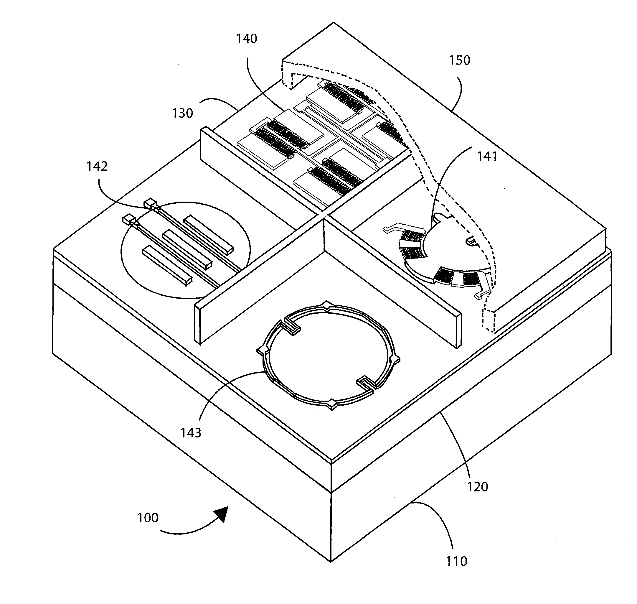
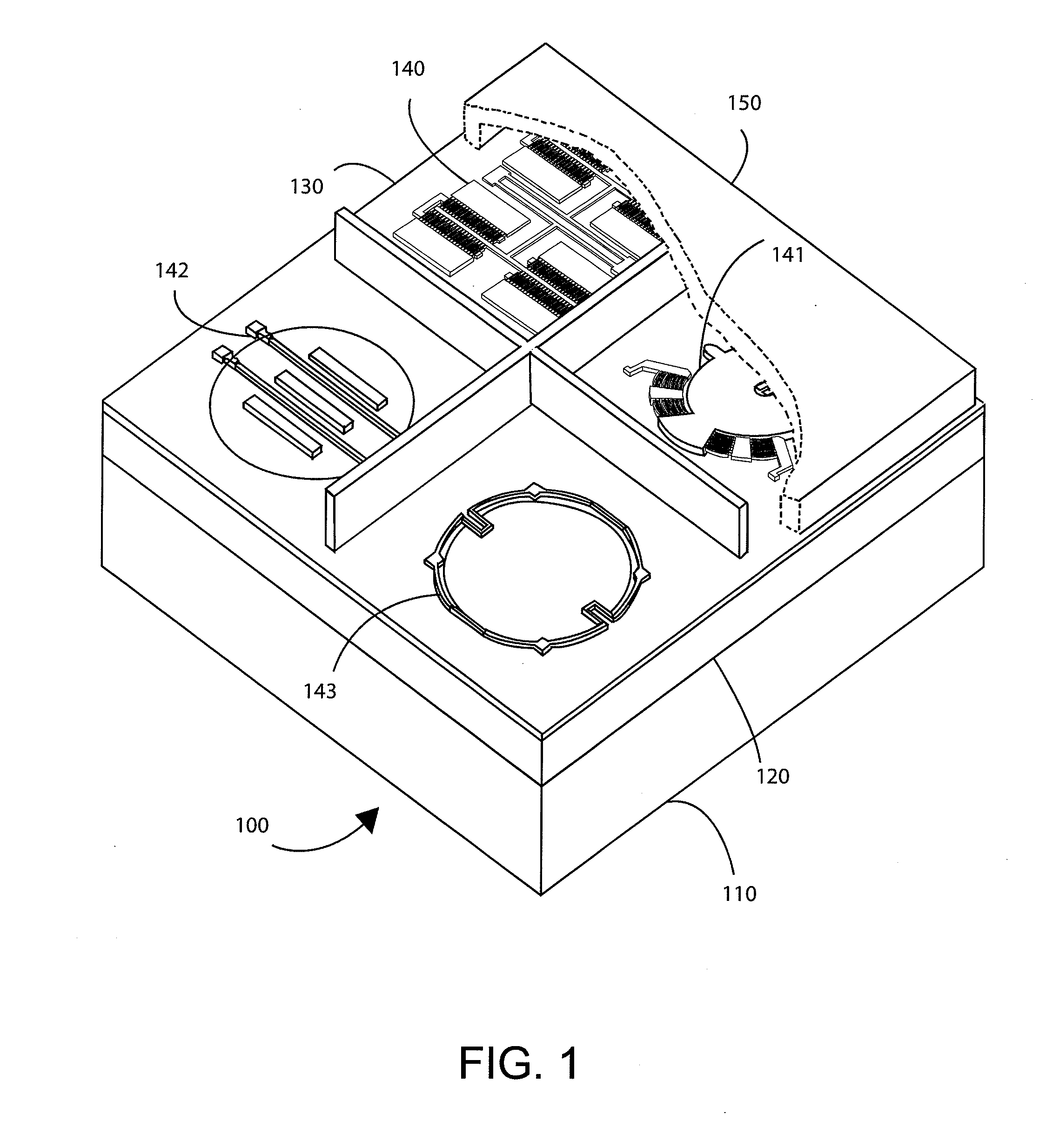
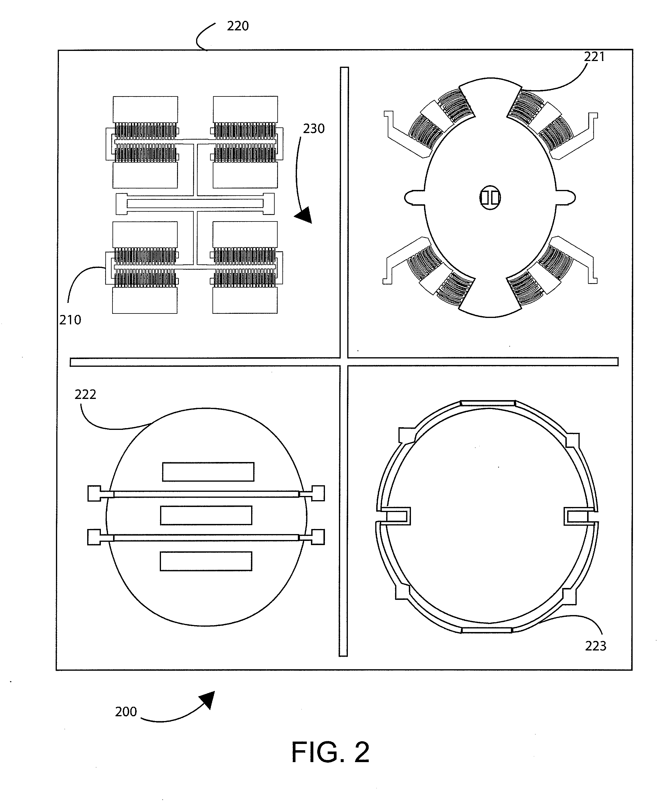
[0023]According to the present invention, techniques related generally to integrated devices and systems are provided. More particularly, the present invention provides systems and methods for integrating one or more MEMS devices with other system applications configured on at least CMOS integrated circuit devices. Merely by way of example, the MEMS devices can include at least an accelerometer, a gyroscope, a magnetic sensor, a pressure sensor, a microphone, a humidity sensor, a temperature sensor, a chemical sensor, a biosensor, an inertial sensor, and others. Additionally, the other applications include at least a sensor application or applications, system applications, and broadband applications, among others.

[0024]FIG. 1 is a simplified perspective diagram of an integrated CMOS-MEMS system according to an embodiment of the present invention. This diagram is merely an example, which should not unduly limit the scope of the claims herein. One of ordinary skill in the art would re...


PUM


Abstract

An integrated MEMS system in which CMOS and MEMS devices are provided to form an integrated CMOS-MEMS system. The system can include a silicon substrate layer, a CMOS layer, MEMS and CMOS devices, and a wafer level packaging (WLP) layer. The CMOS layer can form an interface region, one which any number of CMOS MEMS devices can be configured.

Description

CROSS-REFERENCE TO RELATED APPLICATIONS[0001]The present application claims priority to and incorporates by reference, for all purposes, the following pending patent application: U.S. Patent Application No. 61 / 255,490, filed Oct. 28, 2009. The present invention also incorporates by reference, for all purposes, the following pending patent applications related to sensor and MEMS devices: U.S. patent application Ser. No. 12 / 859,631, filed Aug. 19, 2010; U.S. Patent Application No. 61 / 356,467, filed Jun. 18, 2010; U.S. patent application Ser. No. 12 / 859,672, filed Aug. 19, 2010; and U.S. patent application Ser. No. 12 / 859,647, filed Aug. 19, 2010.BACKGROUND OF THE INVENTION[0002]The present invention relates generally to integrated devices. More particularly, the present invention provides a system and method for integrating at least two different micro electro mechanical systems (MEMS) devices with one or more complementary metal oxide semiconductor (CMOS) devices. Such MEMS devices c...

Claims


Application Information

Patent Timeline
IPC IPC(8): H01L29/84H01L21/56G01H17/00
CPCB81C1/00246B81B2207/015B81C1/00396B81C1/00626B81C2201/0198B81C2203/0136
Inventor YANG, XIAO "CHARLES"
Owner MOVELLA INC
Why Eureka
Try Eureka