Nitride semiconductor device

a semiconductor and nitride technology, applied in the direction of semiconductor devices, basic electric elements, electrical appliances, etc., can solve the problems of buffer layer prone to misfit transition to reduce stress energy, buffer layer fails to serve the intended purpose, and high price of group iii nitride semiconductor substrates

Active Publication Date: 2011-11-10
ROHM CO LTD
View PDF2 Cites 50 Cited by
  • Summary
  • Abstract
  • Description
  • Claims
  • Application Information

AI Technical Summary

Benefits of technology

[0010]It is an object of the present invention to provide a nitride semiconductor device which is substantially free from increase in leak current, and substan...

Problems solved by technology

However, the Group III nitride semiconductor substrate is expensive.
If having a thickness greater than the critical thickness, on the other hand, the buffer layer is liable to experience misfit transition to reduce a stress energy.
As a result, the buffer layer fails to serve for its intende...

Method used


Image

  • Nitride semiconductor device
  • Nitride semiconductor device
  • Nitride semiconductor device

Examples


example 1

(1) Example 1

[0069]First, an AlN layer (having a thickness of 40 nm) was epitaxially grown on a surface of a Si substrate having a (111) plane as its major surface. Then, the step of forming an AlN sublayer (having a thickness of 5 nm) and forming an AlGaN sublayer (having a thickness of 25 nm) on the AlN sublayer was repeatedly performed 60 times, whereby an AlN / AlGaN superlattice layer (including 60 periods of AlN / AlGaN) was formed. In the formation of the AlGaN sublayer, the Al composition ratio of the AlGaN sublayer was controlled to be 20%. The AlN / AlGaN superlattice layer thus formed totally had an average Al composition ratio of 33.3%.

[0070]Subsequently, the step of forming an AlN sublayer (having a thickness of 5 nm) and forming an AlGaN sublayer (having a thickness of 25 nm) on the AlN sublayer was repeatedly performed 20 times, whereby an AlN / AlGaN superlattice layer (including 20 periods of AlN / AlGaN) was formed. In the formation of the AlGaN sublayer, the Al composition ...

example 2

(1) Example 2

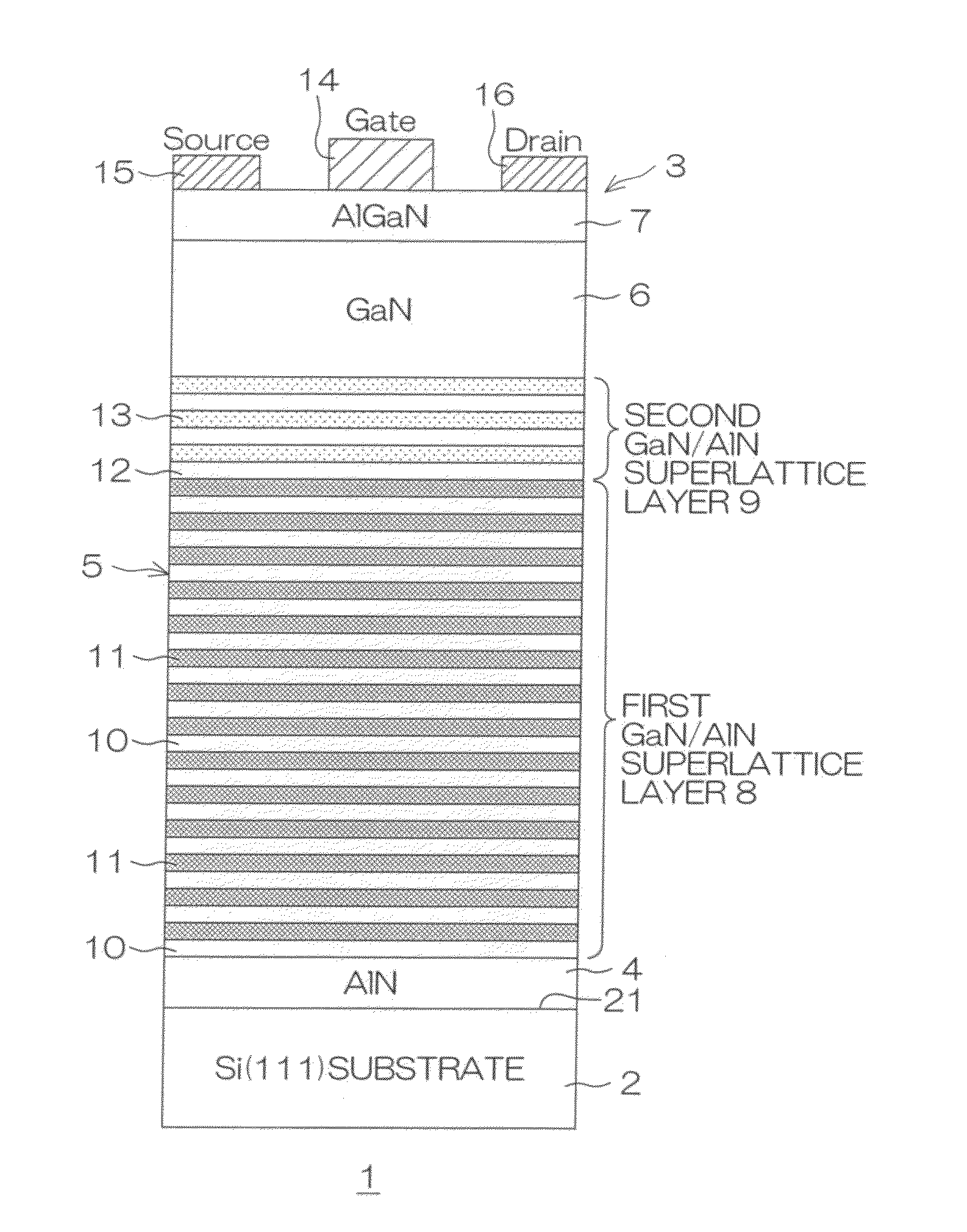
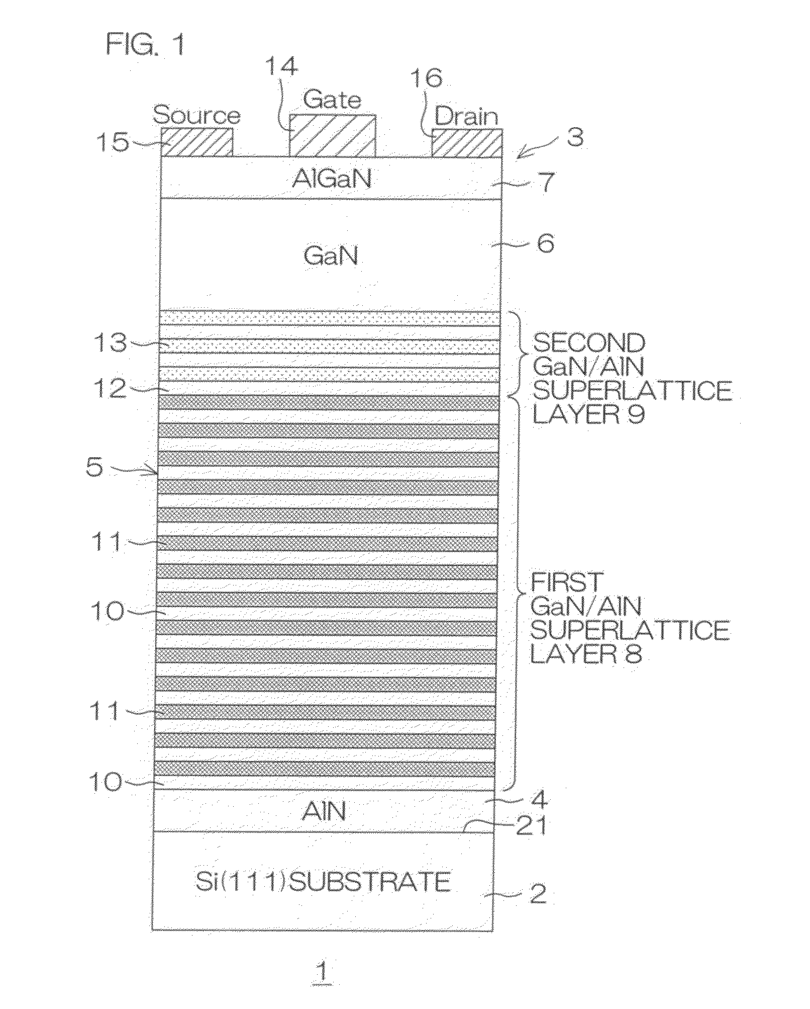
[0082]First, an AlN layer (having a thickness of 100 nm) was epitaxially grown on a surface of a Si substrate (having a thickness of 300 μm) having a (111) plane as its major surface. Then, the step of forming a GaN sublayer (having a thickness of 20 nm) and forming an AlN sublayer (having a thickness of 5 nm) on the GaN sublayer was repeatedly performed 53 times, whereby a GaN / AlN superlattice layer (including 53 periods of GaN / AlN) was formed. The GaN / AlN superlattice layer thus formed totally had an average Al composition ratio of 20%.

[0083]Subsequently, the step of forming a GaN sublayer (having a thickness of 30 nm) and forming an AlN sub layer (having a thickness of 5 nm) on the GaN sublayer was repeatedly performed 11 times, whereby a GaN / AlN superlattice layer (including 11 periods of GaN / AlN) was formed. The GaN / AlN superlattice layer thus formed totally had an average Al composition ratio of 14%.

[0084]Thereafter, a GaN layer (having a thickness of 2.5 μm) and ...


PUM


Abstract

An inventive nitride semiconductor device includes: a substrate; a first buffer layer provided on the substrate, and having a superlattice structure which includes two types of Group III nitride semiconductor sublayers having different compositions and alternately stacked in pairs; a second buffer layer provided on the first buffer layer in contact with the first buffer layer, and having a superlattice structure which includes two types of Group III nitride semiconductor sublayers having different compositions and alternately stacked in pairs; and a device operation layer of a Group III nitride semiconductor provided on the second buffer layer; wherein an average lattice constant LC1 of the first buffer layer, an average lattice constant LC2 of the second buffer layer and an average lattice constant LC3 of the device operation layer satisfy the following expression (1):
LC1<LC2<LC3  (1)

Description

BACKGROUND OF THE INVENTION[0001]1. Field of the Invention[0002]The present invention relates to a nitride semiconductor device employing Group III nitride semiconductors.[0003]2. Description of Related Art[0004]Nitride semiconductor devices such as HEMTs (High Electron Mobility Transistors) and MISFETs (Metal Insulator Semiconductor Field Effect Transistors) which employ Group III nitride semiconductors are known to be used as power devices for power amplifier circuits, motor driving circuits and the like.[0005]Such a nitride semiconductor device is produced, for example, by using an epitaxial wafer including a substrate and an epitaxial layer formed on the substrate by epitaxial growth of a Group III nitride semiconductor. The substrate to be used is preferably of the same type as the epitaxial layer, i.e., a Group III nitride semiconductor substrate, for reduction of a difference in linear expansion coefficient between the substrate and the epitaxial layer.[0006]However, the Grou...

Claims


Application Information

Patent Timeline
IPC IPC(8): H01L29/15
CPCH01L21/02381H01L21/02458H01L21/02507H01L21/0254H01L29/7787H01L29/2003H01L29/452H01L29/475H01L29/66462H01L29/155
Inventor YAMAGUCHI, ATSUSHIITO, NORIKAZUTAKADO, SHINYA
Owner ROHM CO LTD
Why Eureka
Try Eureka