Acoustic sensor and method of manufacturing the same

Active Publication Date: 2011-11-17
MMI SEMICON CO LTD
View PDF41 Cites 15 Cited by
  • Summary
  • Abstract
  • Description
  • Claims
  • Application Information

AI Technical Summary

Benefits of technology

In the manufacturing method of the acoustic sensor according to one or more embodiments of the present invention, the thickness of the protective film can be increased and the insulation properties at the outer peripheral part of the upper surface of the semiconductor substrate can be enhanced because the outer peripheral part of the upper surface of the semiconductor substrate to the outer periphery thereof (end edge) is covered with the protective film having insulation properties made from the same material as the fixed film. Therefore, the bonding wire connected to the electrode terminal is prevented from being bent and brought into contact with the upper surface of the semiconductor substrate and the foreign substance is prevented from being caught between the bonding wire and the upper surface of the semiconductor substrate, and causing short circuit. Furthermore, because the protective film is made from the same material as the fixed film and the protective film can be formed in the same process as the fixed film, the manufacturing man hours of the acoustic sensor does not increase and the productivity does not lower from arranging the protective film.
In the manufacturing method of the acoustic sensor according to one or more embodiments of the present invention, an adhesive layer that is made from a material different from the fixed film and that is thinner than the protective film is formed in at least one part of the outer peripheral part of the upper surface of the semiconductor substrate after forming the space shaping portion. In particular, the thickness of the adhesive layer is smaller than an interval between the inner surface of the back plate including the fixed film and the fixed electrode film, and the diaphragm. Accordingly, the adhesive layer of the thin film thinner than the protective film is formed between the protective film and the semiconductor substrate to reduce the film stress generated at the protective film and alleviate the stripping of the protective film by the film stress. Furthermore, because the adhesive layer is a thin film, the throughput is less likely to lower when forming a plurality of acoustic sensors on a wafer during the manufacturing process and then separating the wafer into individual acoustic sensors by laser dicing at the area where the adhesive layer is formed. The adhesive film is arranged separate from the space shaping portion after forming the space shaping portion, and hence

Problems solved by technology

Furthermore, because the protective film is made from the same material as the fixed film and the protective film can be formed in the same process as the

Method used


Image

  • Acoustic sensor and method of manufacturing the same
  • Acoustic sensor and method of manufacturing the same
  • Acoustic sensor and method of manufacturing the same

Examples


Example

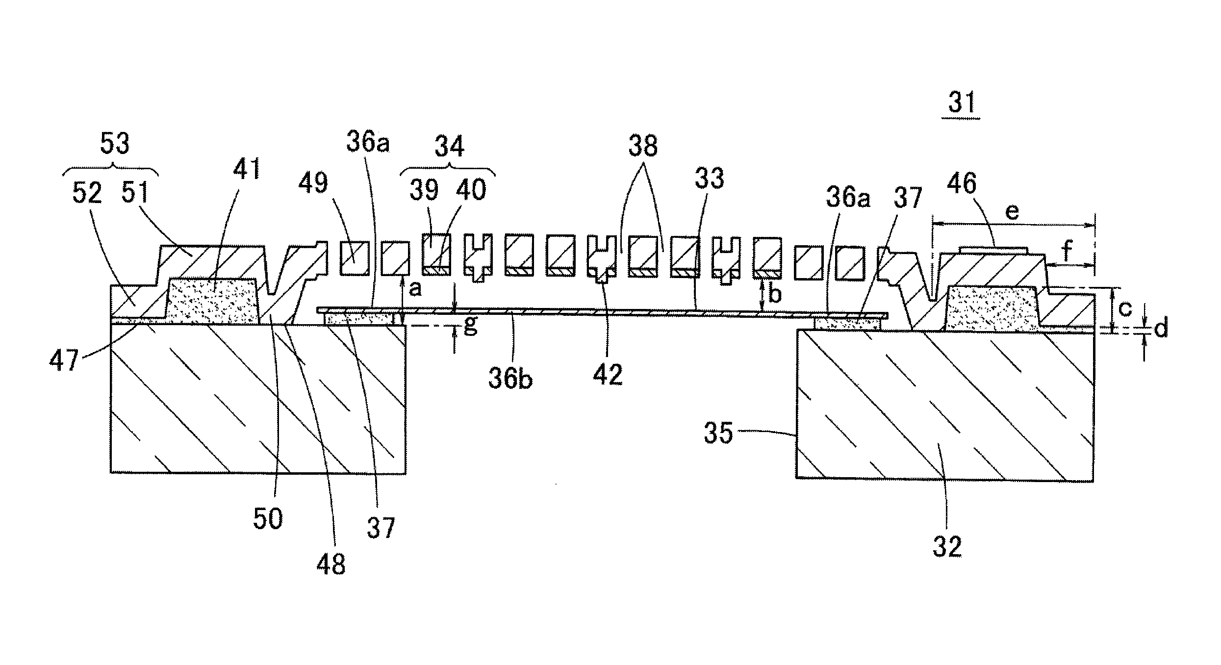
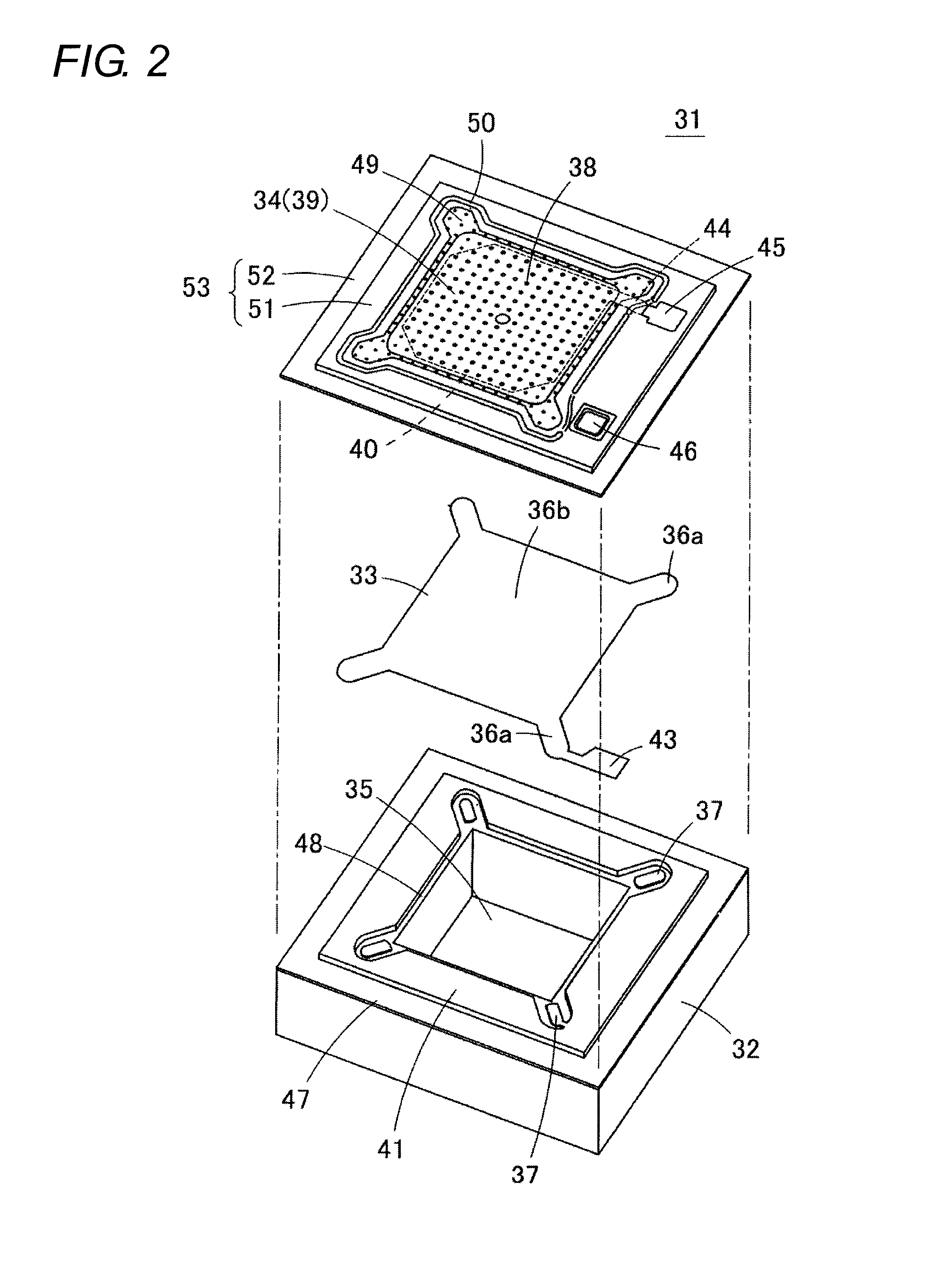
First, a structure of an acoustic sensor 31 according to a first embodiment of the present invention will be described with reference to FIG. 2 and FIG. 3. FIG. 2 is a perspective view showing the acoustic sensor 31 in a partially exploded manner. FIG. 3 is a cross-sectional view in a diagonal direction showing the structure of the acoustic sensor 31.

The acoustic sensor 31 is a microscopic capacitance type element manufactured using the MEMS technique, where a diaphragm 33 is arranged on an upper surface of a silicon substrate 32 (semiconductor substrate) through an anchor 37, and a back plate 34 is fixed thereon through a microscopic gap (void), as shown in FIG. 3.

The silicon substrate 32 is made of a monocrystal silicon. As shown in FIG. 2, the silicon substrate 32 is formed to a rectangular shape, and includes a back chamber 35 having a square hole shape that passes from the front surface to the back surface. The inner peripheral surface of the back chamber 35 may be a perpendicu...


PUM


Abstract

In an acoustic sensor, a diaphragm arranged on an upper side of a silicon substrate includes a back chamber, and an anchor supports the diaphragm. An insulating plate portion fixed to an upper surface of the silicon substrate covers the diaphragm with a gap. A conductive fixed electrode film arranged on a lower surface of the plate portion configures a back plate. The change in electrostatic capacitance between the fixed electrode film and the diaphragm outputs to the outside from a fixed side electrode pad and a movable side electrode pad as an electric signal. A protective film is arranged continuously with the plate portion at an outer periphery of the plate portion. The protective film covers the outer peripheral part of the upper surface of the silicon substrate, and the outer periphery of the protective film coincides with the outer periphery of the upper surface of the silicon substrate.

Description

BACKGROUND OF THE INVENTION1. Technical FieldThe present invention relates to acoustic sensors and methods for manufacturing the same, and specifically to a MEMS (Micro Electro Mechanical Systems) type acoustic sensor manufactured using a MEMS technique, and a method for manufacturing the same.2. Related ArtThe MEMS acoustic sensor is disclosed in Japanese Unexamined Patent Publication Nos. 2008-301434 and 2009-89097, for example.(Regarding Japanese Unexamined Patent Publication No. 2008-301434)FIGS. 1A and 1B are schematic cross-sectional views showing a state in which an acoustic sensor disclosed in FIG. 7 and FIG. 8 of Japanese Unexamined Patent Publication No. 2008-301434 is mounted in a package. The acoustic sensor 11 has a diaphragm 14 (vibration thin film) laminated on a silicon substrate 12 with a back chamber 13 opened, and a back plate 15 arranged on the silicon substrate 12 to cover the diaphragm 14. Such an acoustic sensor 11 is normally mounted in a package 17 along wit...

Claims


Application Information

Patent Timeline
IPC IPC(8): H01L29/84H01L21/02
CPCB81B2201/0257B81B2207/012H04R31/00B81C2201/053H04R19/005B81B7/0016H01L2224/48091H01L2224/48137H01L2224/8592H01L2924/16151H01L2924/00014H04R19/04
Inventor KASAI, TAKASHIIIDA, NOBUYUKINAKAMURA, TOMOFUMI
Owner MMI SEMICON CO LTD
Why Eureka
Try Eureka