Power Electronic Device Package

a technology of electronic devices and power supply, applied in semiconductor devices, semiconductor/solid-state device details, electrical apparatus, etc., can solve the problems of large board footprint, complex integration, and advanced packaging technology, and achieve the effects of improving power handling capability, small footprint, and improving internal chip mounting area

Inactive Publication Date: 2011-11-17
IQXPRZ POWER
View PDF3 Cites 21 Cited by
  • Summary
  • Abstract
  • Description
  • Claims
  • Application Information

AI Technical Summary

Benefits of technology

[0009]The power electronic device package and method for creating the power electronic device package disclosed herein addresses the above stated need for a power electronic device package that is configured as a transfer molded power module with multiple leads and increased power handling capability, and that provides an improved internal chip mounting area, a small footprint, a compact package design, and flexibility in design, where internal chip mounting patterns can be easily changed to suit application needs. The power electronic device package disclosed herein is an alternative to discrete power devices in inverter-based systems and other applications that require a combination of several discrete components in their power circuit sections. Furthermore, the power electronic device package disclosed herein has an increased power handling capability, thereby allowing the use of large electronic chips in a single transistor outline (TO) package. In addition to integration to form a desired specific application power circuit, the power electronic device package disclosed herein also allows paralleling of power electronic devices to achieve, for example, high current rating power switches. The power electronic device package disclosed herein allows a large chip with a high current rating to be mounted in a single package, or a number of chips to be mounted and connected in parallel in a single package.

Problems solved by technology

This requires a large number of components, which produces a bigger board footprint and requires a larger heat sink.
Advanced packaging technology involving packaging of a power device gate drive, a control circuit, and a protection circuit in some cases, requires more complex integration.
The existing power semiconductor packages, for example, existing transistor outline (TO) packages such as the TO247 packages, offer limited current handling capability to cater to medium to high power application requirements.
Conventionally, a number of devices packaged in separate TO247 packages are mounted in an array form to enable paralleling of their external leads, which is disadvantageous.

Method used


Image

  • Power Electronic Device Package
  • Power Electronic Device Package
  • Power Electronic Device Package

Examples


Embodiment Construction

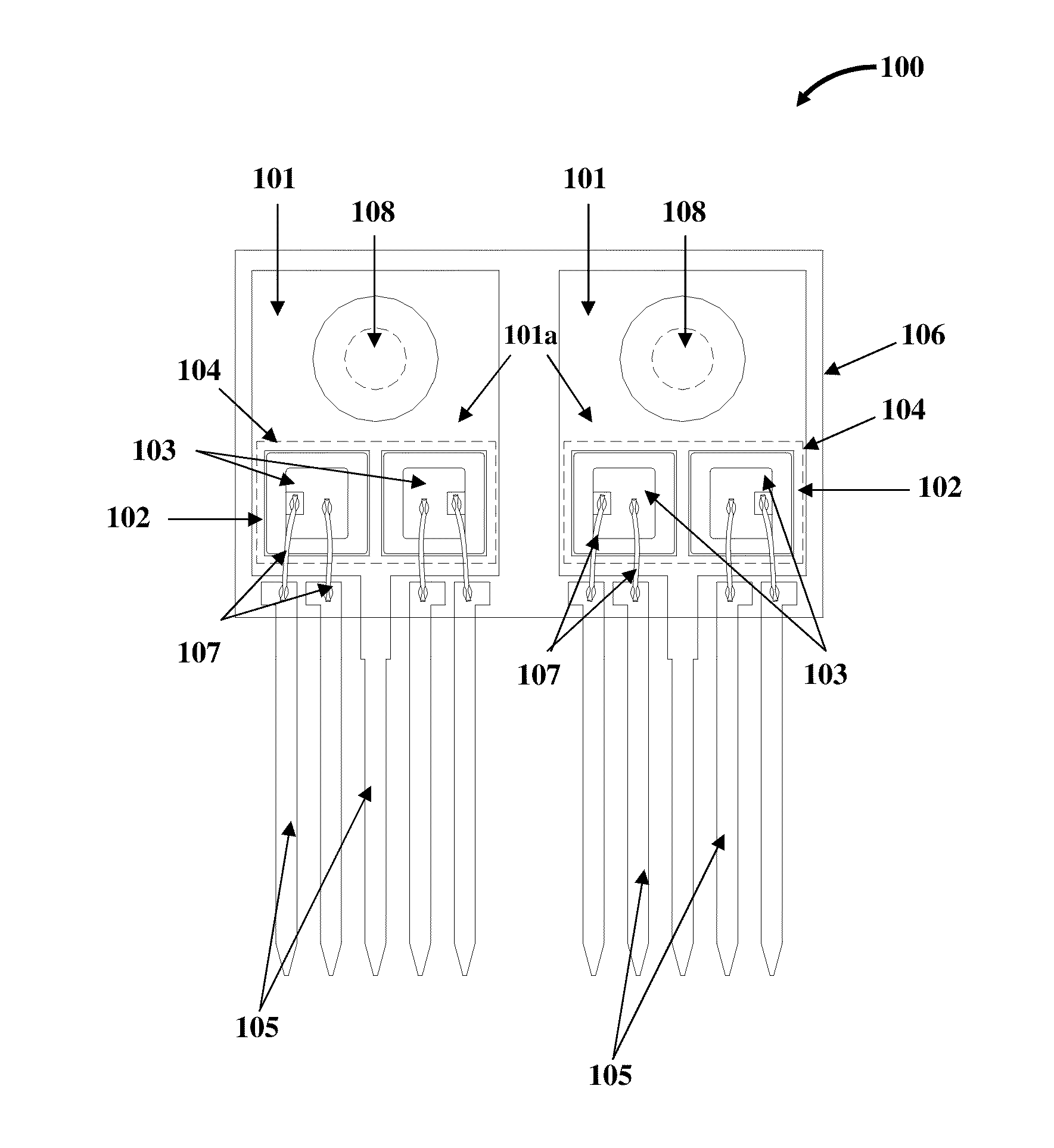
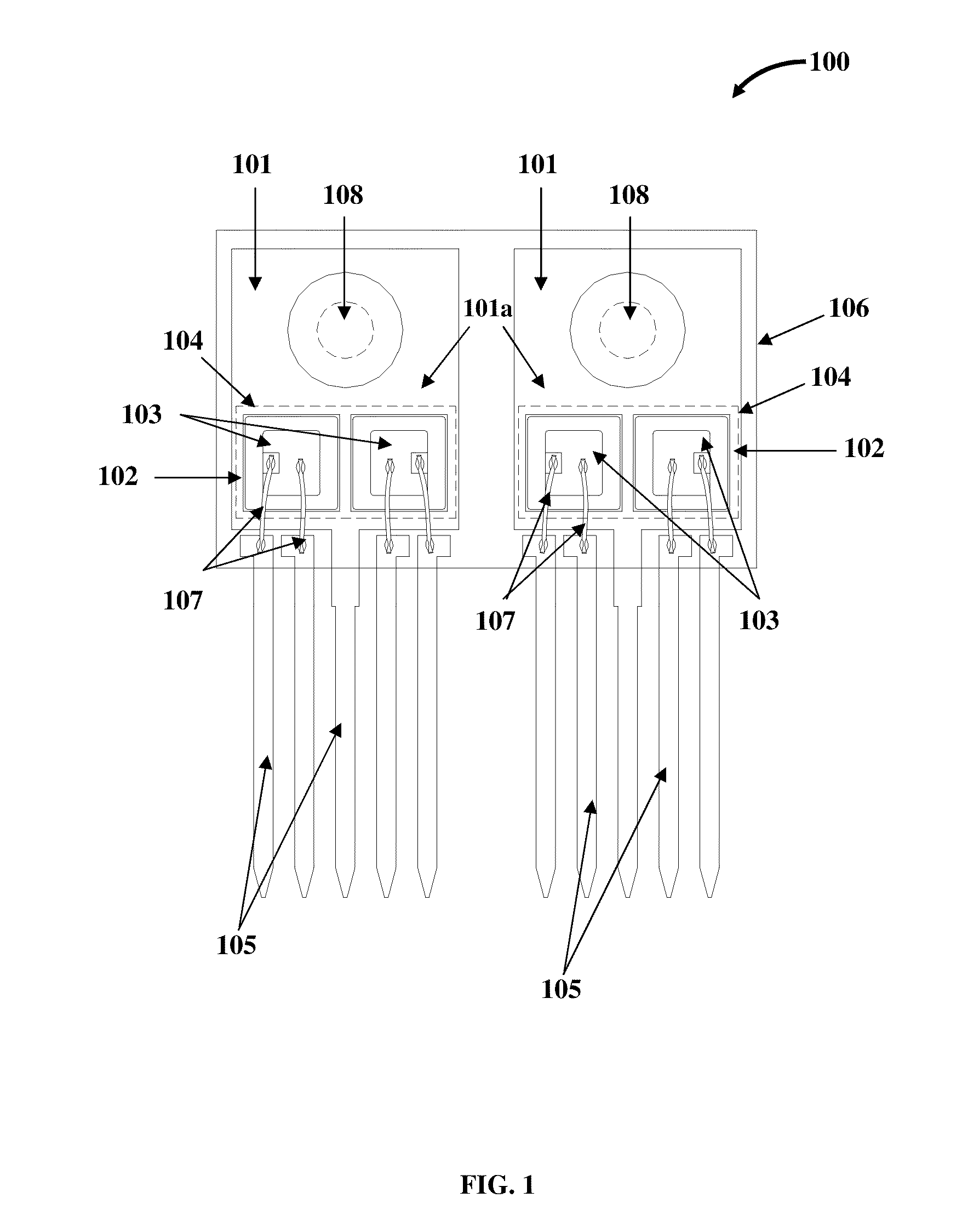
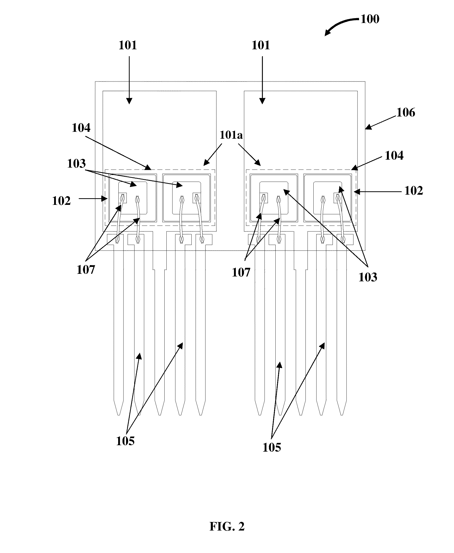
[0036]FIG. 1 and FIG. 2 exemplarily illustrate orthogonal views of a power electronic device package 100 with and without mounting holes 108 respectively, showing power electronic devices 103 directly mounted on the base member 101. The power electronic device package 100 disclosed herein is configured, for example, as a multiple leads expanded transistor outline (TO) package, that is, a multiple leads expanded TO247 package. The power electronic device package 100 disclosed herein comprises a base member 101, a device layer 102, multiple leads 105, and an encapsulant 106.

[0037]The base member 101 is thermally conductive for heat dissipation. As used herein, the term “base member” refers to, for example, a copper base member, a direct copper bonded (DCB) substrate, a combination of the copper base member and the direct copper bonded substrate, an intermetallic substrate (IMS), a plastic molded copper base member, etc. The base member 101 disclosed in the detailed description of FIGS...


PUM


Abstract

A power electronic device package comprising a base member, a device layer, multiple leads, and an encapsulant is provided. The base member is thermally conductive for heat dissipation. The device layer comprises one or more power electronic devices mounted on the base member. The power electronic devices are selectively electrically connected to each other and to the base member to form an internal electronic circuit. The leads extend outwardly from the base member and are electrically connected to the internal electronic circuit. The encapsulant encases the internal electronic circuit, a portion of the base member, and a portion of the leads. The power electronic device package is configured as a transfer molded power module with multiple leads and increased power handling capability. In an embodiment, the base member is electrically conductive to operate as an electrical terminal. The base member may also be isolatably connected to the internal electronic circuit.

Description

CROSS REFERENCE TO RELATED APPLICATIONS[0001]This application claims the benefit of provisional patent application No. 61 / 333,277 titled “Power Electronic Device Package”, filed on May 11, 2010 in the United States Patent and Trademark Office.[0002]The specification of the above referenced patent application is incorporated herein by reference in its entirety.BACKGROUND[0003]Semiconductor technology continues to advance rapidly, producing smaller and more efficient devices that challenge the packaging and assembly technology for accommodating complex configurations in a single package with improved layouts and designs, without compromising quality and efficiency.[0004]The use of inverters in various applications is now common due to significant energy savings over non-inverter based designs. There is a need for inverter based systems that are more compact, reliable, and that have lower overall costs.[0005]There are several methods of designing a power circuit for different applicati...

Claims


Application Information

Patent Timeline
Patent Type & Authority Applications(United States)
IPC IPC(8): H01L23/495H01L21/98H01L23/52
CPCH01L23/4334H01L2224/49111H01L23/49537H01L23/49548H01L23/49562H01L23/49568H01L23/49575H01L2224/48137H01L2224/48247H01L2224/48472H01L2924/01079H01L24/48H01L2924/01327H01L23/49531H01L2224/0603H01L2224/45144H01L2224/45124H01L2924/00H01L2224/48139H01L2224/45147H01L2224/45014H01L2924/00014H01L24/45H01L2924/181H01L2224/49431H01L24/49H01L2224/05599H01L2924/00012H01L2924/206
Inventor HERRAS, EMMANUEL ORPIA
Owner IQXPRZ POWER
Why Eureka
Try Eureka