

Method for manufacturing group iii nitride semiconductor layer, method for manufacturing group iii nitride semiconductor light-emitting device, and group iii nitride semiconductor light-emitting device, and lamp
a technology of nitride and semiconductor, which is applied in the direction of solid-state devices, vacuum evaporation coatings, coatings, etc., can solve the problem of inability to perform an additional test by third parties, and achieve the effect of easy control of the electric resistance in the group iii nitride layer, and easy control of the amount of si
Inactive Publication Date: 2011-11-24
TOYODA GOSEI CO LTD
View PDF3 Cites 2 Cited by
- Summary
- Abstract
- Description
- Claims
- Application Information
AI Technical Summary
Benefits of technology
This method enables the formation of Group III nitride semiconductor layers with optimized electric resistance and crystallinity, achieving high doping efficiency and excellent light emission properties.
Problems solved by technology
Non-Patent Document 3 does not describe a specific doping method and therefore it is impossible to perform an additional test by third party.
Method used
View moreImage
Smart ImageViewing Examples

Examples
examples
[0207]The present invention will be described in more detail by way of Example, but the present invention is not limited only to these Examples.
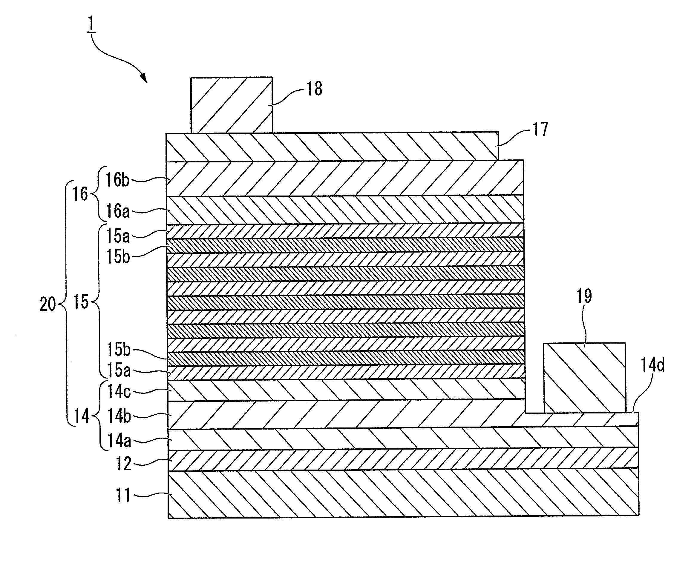
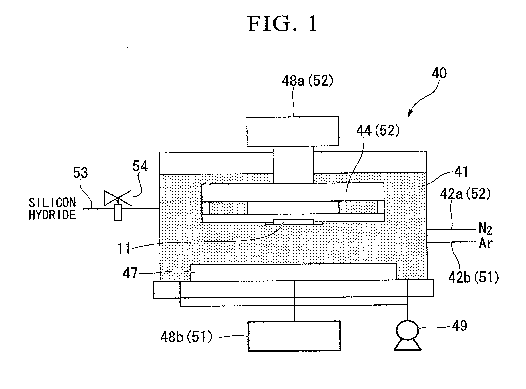
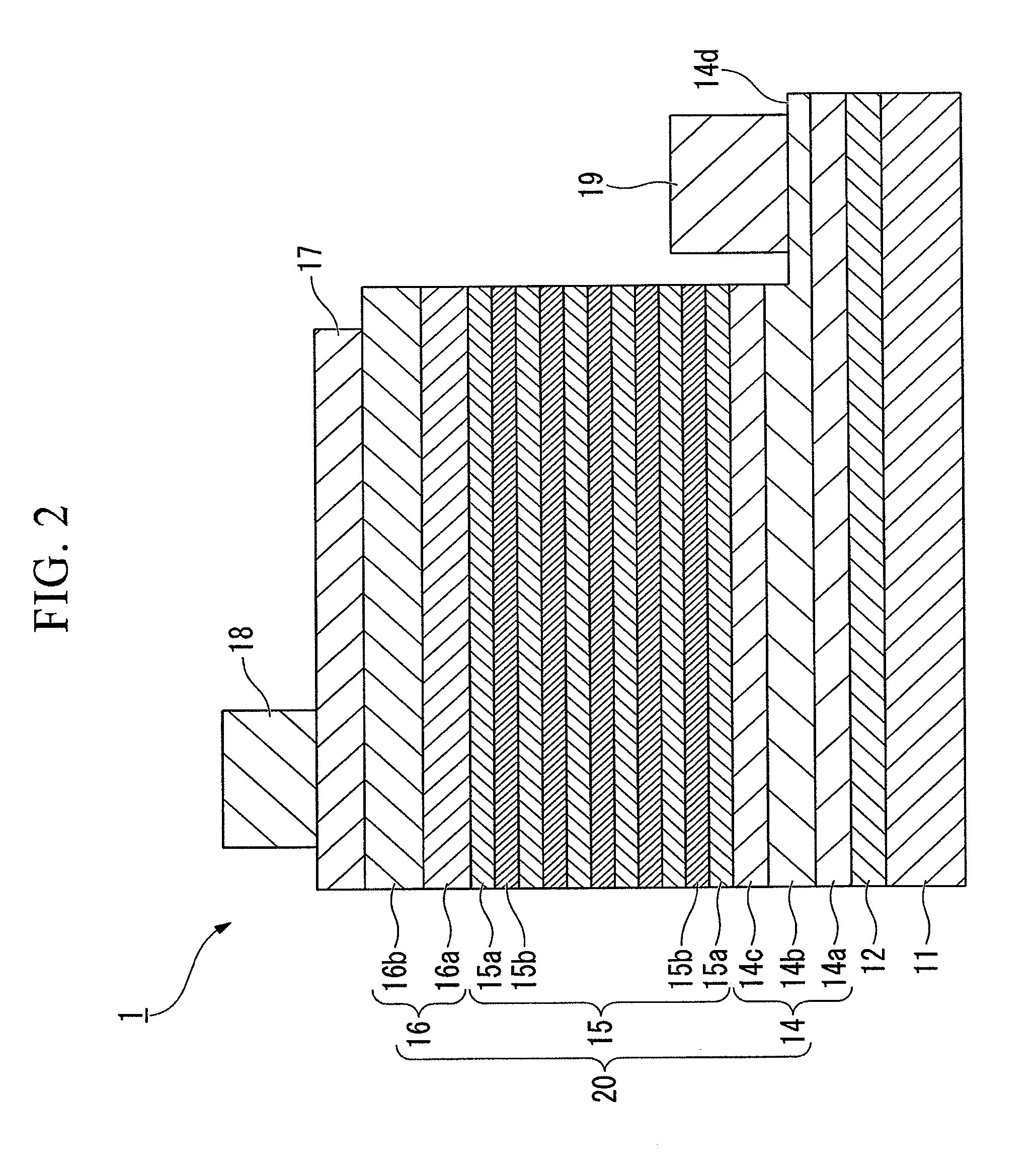
[0208]In order to examine a relation between the flow rate of a silane gas (SiH4) and the amount of Si, with which a GaN layer is doped, an n-type semiconductor layer 14 shown in FIG. 4 was formed in the following manner using a manufacturing method using a sputtering apparatus 40 shown in FIG. 1.
Login to View More PUM
| Property | Measurement | Unit |
|---|---|---|
| thickness | aaaaa | aaaaa |
| thickness | aaaaa | aaaaa |
| thickness | aaaaa | aaaaa |
Abstract
A method for manufacturing a Group III nitride semiconductor layer according to the present invention includes a sputtering step of disposing a substrate and a target containing a Group III element in a chamber, introducing a gas for formation of a plasma in the chamber and forming a Group III nitride semiconductor layer added with Si as a dopant on the substrate by a reactive sputtering method, wherein a Si hydride is added in the gas for formation of a plasma.
Description
CROSS-REFERENCE TO RELATED APPLICATIONS[0001]This is a Rule 53(b) Continuation of application Ser. No. 12 / 922,135 filed Sep. 10, 2010, which is a 371 of PCT Application No. PCT / JP2009 / 054436 filed Mar. 9, 2009, and which claims benefit to Japanese Patent Application No. 2008-062597 filed Mar. 12, 2008. The above-noted applications are incorporated herein by reference in their entirety.TECHNICAL FIELD[0002]The present invention relates to a method for manufacturing a Group III nitride semiconductor layer that is suitable for use in a light-emitting diode (LED), a laser diode (LD), an electronic device, or the like, and particularly to a method for manufacturing a Group III nitride semiconductor layer that is used for formation of a Group III nitride semiconductor layer in which a dopant has been added, a method for manufacturing a Group III nitride semiconductor light-emitting device, and a Group III nitride semiconductor light-emitting device, and a lamp.BACKGROUND ART[0003]A Group ...
Claims
Login to View More Application Information
Patent Timeline
 Patent Type & AuthorityApplications(United States)
IPC IPC(8): H01L33/30H01L33/40C23C14/06H01L21/203H01L33/06H01L33/32H01L33/42
CPCC23C14/0617H01L21/0237H01L2224/73265H01L2224/49107H01L2224/48257H01L2224/48247H01L2224/48091H01L2224/32245H01L33/007H01L21/02631H01L21/02576H01L21/02458H01L21/0254H01L2924/00014H01L2924/00H01L2924/181H01L2924/00012
InventorYOKOYAMA, YASUNORIMIKI, HISAYUKI
OwnerTOYODA GOSEI CO LTD