Ohmic electrode and method of forming the same

a technology of ohmic electrode and semiconductor element, which is applied in the direction of basic electric elements, electrical apparatus, and semiconductor devices, can solve the problems of poor wettability between al melt and sic semiconductor, melt agglutinate, etc., and achieve good ohmic characteristic, high surface smoothness, and good ohmic characteristic

Inactive Publication Date: 2011-11-24
TOYOTA JIDOSHA KK
View PDF3 Cites 5 Cited by
  • Summary
  • Abstract
  • Description
  • Claims
  • Application Information

AI Technical Summary

Benefits of technology

[0019]According to the above-described aspect, it is possible to form the ohmic electrode of the p-type SiC semiconductor element, which includes the ohmic electrode layer that is made of Ti3SiC2, and that has high surface smoothness and a good ohmic characteristi

Problems solved by technology

Because wettability between the Al melt and the SiC semiconductor is poor (that is, a contact ang

Method used


Image

  • Ohmic electrode and method of forming the same
  • Ohmic electrode and method of forming the same
  • Ohmic electrode and method of forming the same

Examples


first example

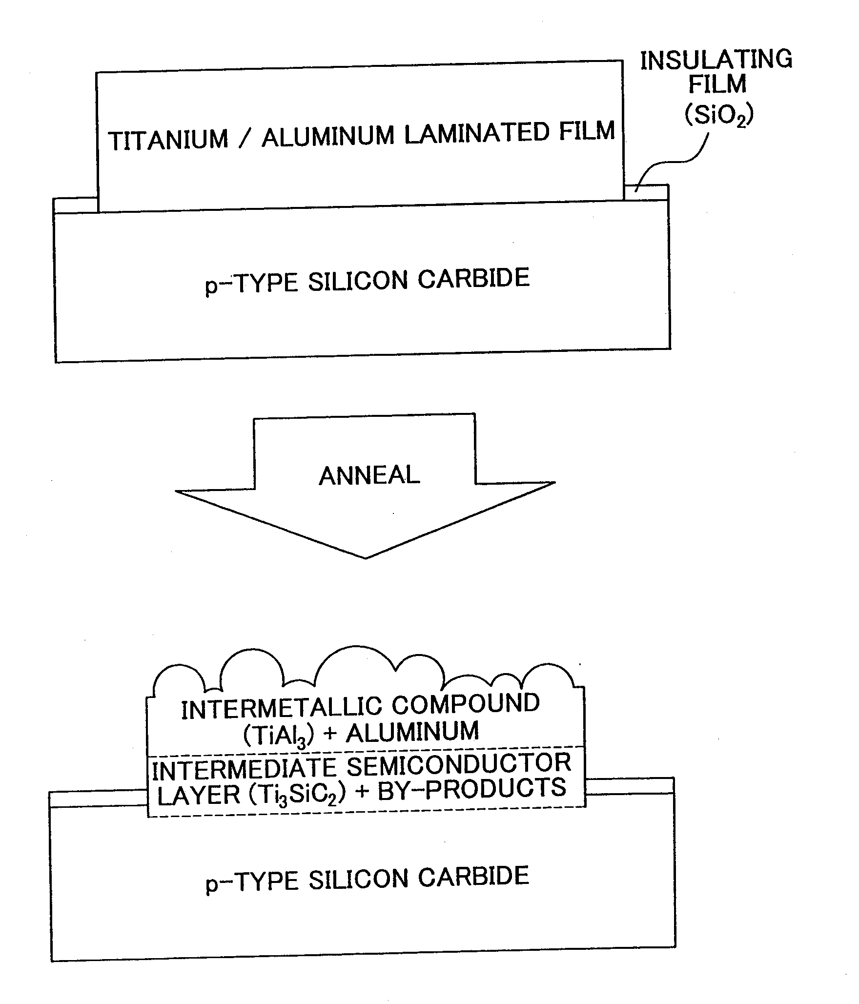
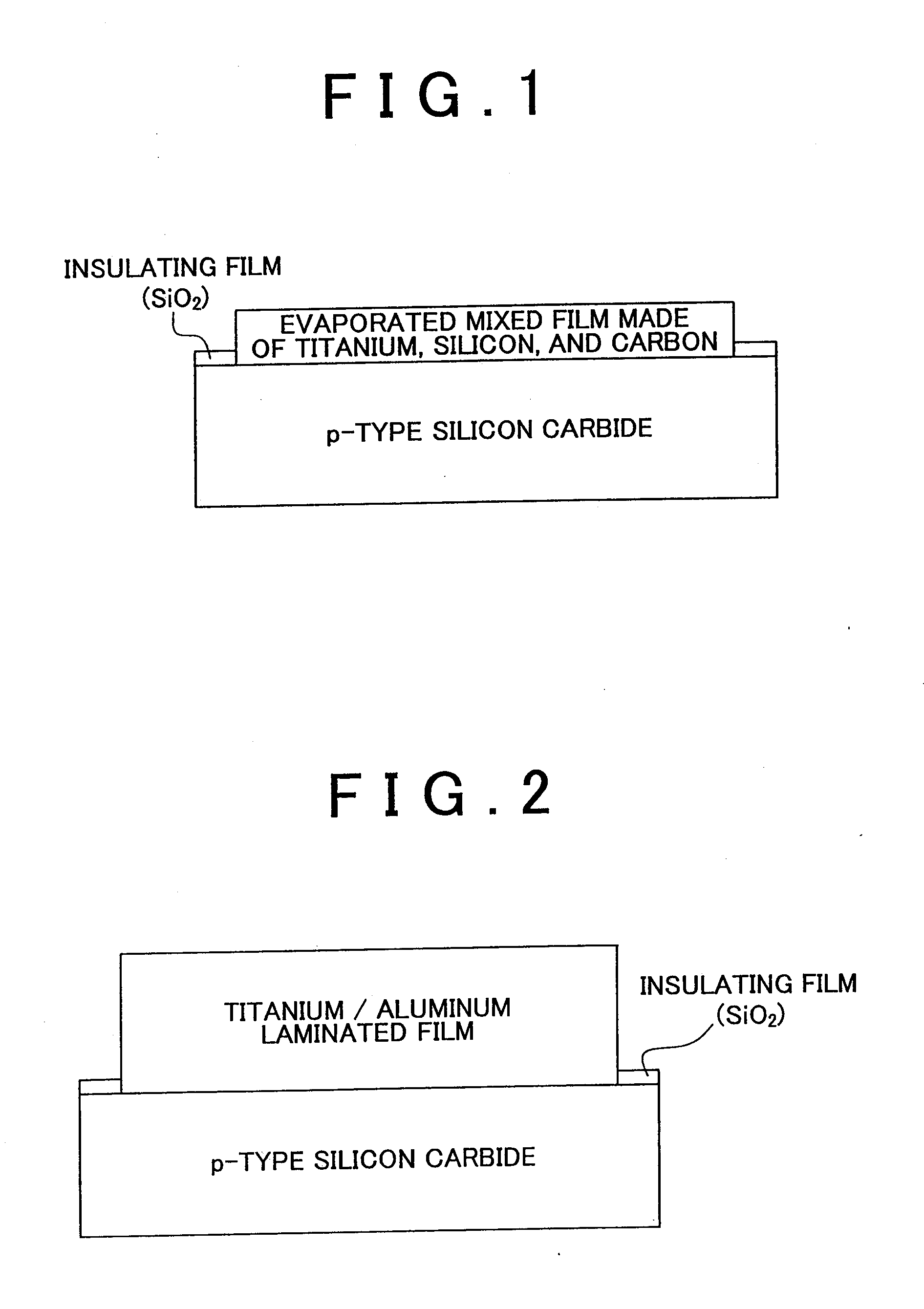
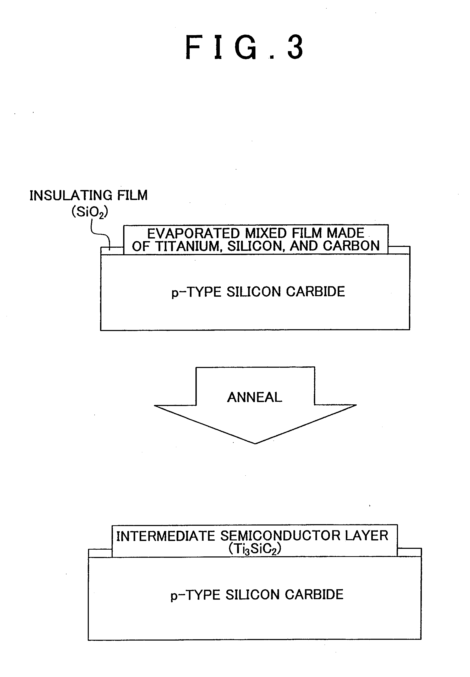
[0042]An evaporated film was formed using a semiconductor substrate made of p-type 4H—SiC. The semiconductor substrate made of p-type 4H—SiC had a thickness of 369 μm, resistivity of 75 to 2500 Ω cm, and a plane inclined from a plane (0001) by an off-angle of 8° toward a [11-20] direction. An electrode was to be formed on an Si surface of the semiconductor substrate. The evaporated film was formed under the condition described below. Radio-frequency magnetron sputtering equipment was used as deposition equipment. Powder, lumps, or compacts of Ti, Si, and C (the composition ratio (the atomic composition ratio), Ti:Si:C=3:1:2) were used as sputtering targets. The evaporation condition was as follows. Before the Ti—S—C film was deposited, the substrate was cleaned by an ordinary method. The evaporation was performed under the Ar discharge atmosphere, at the output of 200 W in the Ar forward direction, for a discharge time of 360 seconds. The evaporated ternary mixed film, which include...

second example

[0048]FIG. 7 is a schematic diagram showing a field-effect transistor which is made of SiC, and which is produced using the ohmic electrode of the p-type SiC semiconductor element according to the invention.

third example

[0049]FIG. 8 is a schematic diagram showing an N-channel power field-effect transistor (a power MOSFET) that is produced using the ohmic electrode of the p-type SiC semiconductor element according to the invention.


PUM


Abstract

The invention provides an ohmic electrode of a p-type SiC semiconductor element, which includes an ohmic electrode layer that is made of Ti3SiC2, and that is formed directly on a surface of a p-type SiC semiconductor. The invention also provides a method of forming an ohmic electrode of a p-type SiC semiconductor element. The ohmic electrode includes an ohmic electrode layer that is made of Ti3SiC2, and that is formed directly on a surface of a p-type SiC semiconductor. The method includes forming a ternary mixed film that includes Ti, Si, and C in a manner such that an atomic composition ratio, Ti:Si:C is 3:1:2, on a surface of a p-type SiC semiconductor to produce a laminated film; and annealing the produced laminated film under vacuum or under an inert gas atmosphere.

Description

BACKGROUND OF THE INVENTION[0001]1. Field of the Invention[0002]The invention relates to an ohmic electrode of a p-type SiC semiconductor element and a method of forming the same. More specifically, the invention relates to an ohmic electrode of a p-type SiC semiconductor element, which includes an ohmic electrode layer made of Ti3SiC2, which has improved surface smoothness, and which is formed directly on a p-type SiC semiconductor, and a method of forming the same.[0003]2. Description of the Related Art[0004]SiC single crystal is extremely stable thermally and chemically, has high mechanical strength, and is resistant to radiation. Further, as compared to Si (silicon) single crystal, the SiC signal crystal has excellent physical properties, such as high breakdown voltage, and high thermal conductivity. Further, it is easy to electronically control the conductivity type of the SiC single crystal to p-type conductivity or n-type conductivity by adding a dopant to the SiC single crys...

Claims


Application Information

Patent Timeline
IPC IPC(8): H01L21/283
CPCH01L21/0485H01L29/45H01L29/1608
Inventor SEKI, AKINORISUGIMOTO, MASAHIROKAWAHASHI, AKIRATAKAHASHI, YASUOMAEDA, MASAKATSU
Owner TOYOTA JIDOSHA KK
Why Eureka
Try Eureka