Array substrate and method of fabricating the same

a technology of array substrate and substrate layer, which is applied in the direction of semiconductor/solid-state device manufacturing, semiconductor devices, electrical devices, etc., can solve the problems of poor adhesion, complex masking process, and negative effects on the performance of thin film transistors, so as to reduce manufacturing processes and costs

Active Publication Date: 2011-12-01
LG DISPLAY CO LTD
View PDF2 Cites 25 Cited by
  • Summary
  • Abstract
  • Description
  • Claims
  • Application Information

AI Technical Summary

Benefits of technology

[0027]An object of the present invention is to provide an array substrate including an oxide semiconductor layer and a method of fabricating the same that prevent the oxide semiconductor layer from being damaged by an etchant for patterning a metal layer and reduce the manufacturing processes and costs.

Problems solved by technology

The characteristics and performance of the thin film transistor may be negatively affected.
However, in the thin film transistor Tr having the oxide semiconductor layer 61 on the source and drain electrodes 57 and 59, which are formed of a metallic material, there may be a problem such as poor adhesion.
Thus, each mask process is complicated and many chemical solutions are used.
As such, as the number of mask processes in the mask method increases, the manufacturing time lengthens.
Therefore, in the related art method and device, the productivity is lowered, more defects are generated, and the manufacturing costs are raised.

Method used


Image

  • Array substrate and method of fabricating the same
  • Array substrate and method of fabricating the same
  • Array substrate and method of fabricating the same

Examples


first embodiment

[0043]FIGS. 4A to 4I are cross-sectional views of illustrating a formation of an array substrate including a thin film transistor with an oxide semiconductor layer according to the present invention. The array substrate shown in FIGS. 4A-4I or in the subsequent figures corresponds to an array substrate of a liquid crystal display device or of an organic electroluminescent display device, but can be an array substrate in other types of devices. The array substrate includes a plurality of thin film transistors each with an oxide semiconductor layer according to the invention. In this regard, FIGS. 4A to 4I show a pixel region including such a thin film transistor. For convenience of explanation, a region for the thin film transistor is defined as a switching region TrA.

[0044]In FIG. 4A, a first metal layer is formed on a transparent insulating substrate 101 by depositing a first metallic material and then is patterned through a mask process, thereby forming a gate line and a gate elec...

second embodiment

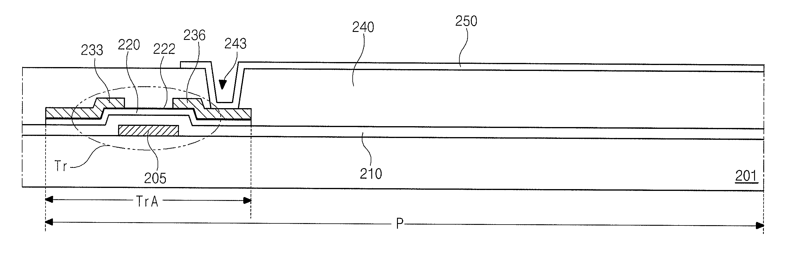
[0081]Next, a transparent conductive material layer is formed on the passivation layer 240 having the drain contact hole 243 by depositing a transparent conductive material, for example, indium tin oxide (ITO) or indium zinc oxide (IZO) on a substantially entire surface of the structure including the substrate 201. The transparent conductive material layer is patterned through a mask process, thereby forming a pixel electrode 250 in the pixel region P. The pixel electrode 250 contacts the drain electrode 236 through the drain contact hole 243. Accordingly, the array substrate according to the present invention is completed.

[0082]The above-mentioned array substrate according to the second embodiment is manufactured by using four (4) mask processes: a first mask process is used for forming the gate electrode, a second mask process is used for forming the oxide semiconductor layer, the etch-prevention layer, and the source and drain electrodes, a third mask process is used for forming ...


PUM


Abstract

A method of fabricating an array substrate and a display device including the array substrate are discussed. According to an embodiment, the method includes forming a gate electrode on a substrate, forming a gate insulating layer on the gate electrode, forming an oxide semiconductor layer and an etch prevention layer on the gate insulating layer using a single mask, forming source and drain electrodes on the etch prevention layer, and forming a passivation layer including a contact hole on the source and drain electrodes and on the gate insulating layer, and forming a pixel electrode on the passivation layer and through the contact hole.

Description

[0001]This application claims the priority benefit of Korean Patent Application No. 10-2010-0050457, filed on May 28, 2010, which is hereby incorporated by reference in its entirety.BACKGROUND OF THE INVENTION[0002]1. Field of the Invention[0003]The present invention relates to an array substrate, and more particularly, to an array substrate including a thin film transistor with an oxide semiconductor layer and a method of fabricating the same.[0004]2. Discussion of the Related Art[0005]With rapid development of information technologies, display devices for displaying a large amount of information have been promptly developed. More particularly, flat panel display (FPD) devices having a thin profile, light weight and low power consumption such as organic electroluminescent display (OLED) devices and liquid crystal display (LCD) devices have been actively pursued and are replacing the cathode ray tubes (CRTs).[0006]Among the liquid crystal display devices, active matrix type liquid c...

Claims


Application Information

Patent Timeline
Patent Type & Authority Applications(United States)
IPC IPC(8): H01L33/02
CPCH01L27/1214H01L27/1225H01L29/7869H01L27/127H01L27/1288H01L29/66969H01L27/1248
Inventor RYOO, CHANG-ILSEO, HYUN-SIKBAE, JONG-UK
Owner LG DISPLAY CO LTD
Why Eureka
Try Eureka