Flip-chip GAN LED fabrication method

a fabrication method and chip technology, applied in semiconductor/solid-state device manufacturing, electrical equipment, semiconductor devices, etc., can solve the problems of affecting the reliability and lifespan of sapphire substrate-based led chips, poor heat transfer characteristics of sapphire substrates, and lowering luminous efficiency, so as to avoid interference, reduce forward voltage and power consumption, and avoid light loss

Inactive Publication Date: 2011-12-01
ENERLIGHTING CORP
View PDF6 Cites 38 Cited by
  • Summary
  • Abstract
  • Description
  • Claims
  • Application Information

AI Technical Summary

Benefits of technology

[0016]As the first isolation protection layer and the metallic reflection layer are respectively formed at two opposite sides relative to the isolation protection layer, the translucent conducting layer and the metallic reflection layer are electrically isolated to minimize forward voltage and power consumption during electricity conduction operation of the metallic reflection layer, avoiding interference with the light-emitting efficiency of the GaN LED chip. Further, the metallic reflection layer is directly mounted inside the GaN LED chip for direct reflection, avoiding light loss.
[0017]Further, subject to the formation of the first groove and the second groove in the GaN epitaxial layer by etching to expose a part of the N-type GaN ohmic contact layer of the GaN epitaxial layer and to divide the GaN epitaxial layer into two epitaxial layer portions, the posteriorly formed P-type electrode pad and N-type electrode pad have the same elevation, stabilizing electric connection between the GaN LED chip and the thermal substrate and improving LED module yield rate.
[0018]Further, the first isolation protection layer and the second isolation protection layer are formed on the two epitaxial layer portions at two opposite sides relative to the second groove, and therefore, the two epitaxial layer portions are well isolated and protected, avoiding a short circuit and enhancing operation reliability.
[0019]Further, the third groove is formed in the first isolation protection layer and the second isolation protection layer adjacent to the metallic reflection layer by etching to expose one lateral side of the N-type electrode pad so that the applied conducting material can climb over the N-type electrode pad into the third groove and be accumulated and cured therein, enhancing the binding strength and the strength of solidification and the connection stability between the N-type electrode pad of the GaN LED chip and the negative solder pad of the thermal substrate.
[0020]Further, the GaN LED chip is electrically connected with the thermal substrate by means of the large area conducting material, and the insulative adhesive is bonded to the thermal substrate between the positive solder pad and the negative solder pad so that the second isolation protection layer can be fixedly secured to the thermal substrate between the positive solder pad and the negative solder pad by means of the conducting material, saving the manufacturing cost, facilitating heat dissipation, improving the luminous efficiency of the GaN LED chip and its lifespan.

Problems solved by technology

However, a sapphire substrate has the drawback of poor heat transfer characteristic.
Temperature will affect he reliability and lifespan of sapphire substrate-based LED chips.
During operation of a conventional LED device, waste heat will be accumulated in the inside of the LED device, lowering the luminous efficiency and shortening the lifespan.
An overheat may result in device burnout.
If waste heat cannot be quickly dissipated during operation of a LED package product, the life cycle and reliability of the product will be badly affected.
However, the use of these attached devices relatively increases the product size, reducing the advantages of small size and light weight of LED products.
However, the use of the metallic P-type electrode pad B6 and N-type electrode pad B8 to reflect light tends to cause an increase of the forward voltage, lowering the luminous efficiency.
This method has the drawback of high manufacturing cost.
As the electrode pads in the flip-chip LED device are electrically connected to the circuit board and capable of reflecting the light emitted by the light-emitting layer toward the sapphire substrate, the metallic property of the electrode pads tends to cause an increase in the forward voltage, thereby lowering the luminous efficiency.
This prior art design discloses the formation of a metallic reflection layer on the circuit board, however, the far distance between the metallic reflection layer and the light-emitting layer causes an attenuation of the emitted light.
However, it is difficult to form the polyimide insulation layer D9 without affecting the relative surface elevation between the electrodes D7 and the conducting metallic reflection layer D6.
A significant elevational difference between the electrodes D7 and the conducting metallic reflection layer D6 will lead to a connection error between the LED and the circuit board, lowering the yield rate.
Further, this design does not teach any measure to protect the surface of the edge of the grooves in the LED chip.
Further, the aforesaid prior art designs cannot eliminate accumulation of waste heat to lower the luminous efficiency due to high consumption of power.
The use of polyimide insulation layer to minimize power consumption relatively lowers heat dissipation performance.
Further, if the P-type electrode pad and the N-type electrode pad are not maintained at the same elevation, circuit board connection may fail, lowering the yield rate.

Method used


Image

  • Flip-chip GAN LED fabrication method
  • Flip-chip GAN LED fabrication method
  • Flip-chip GAN LED fabrication method

Examples


Embodiment Construction

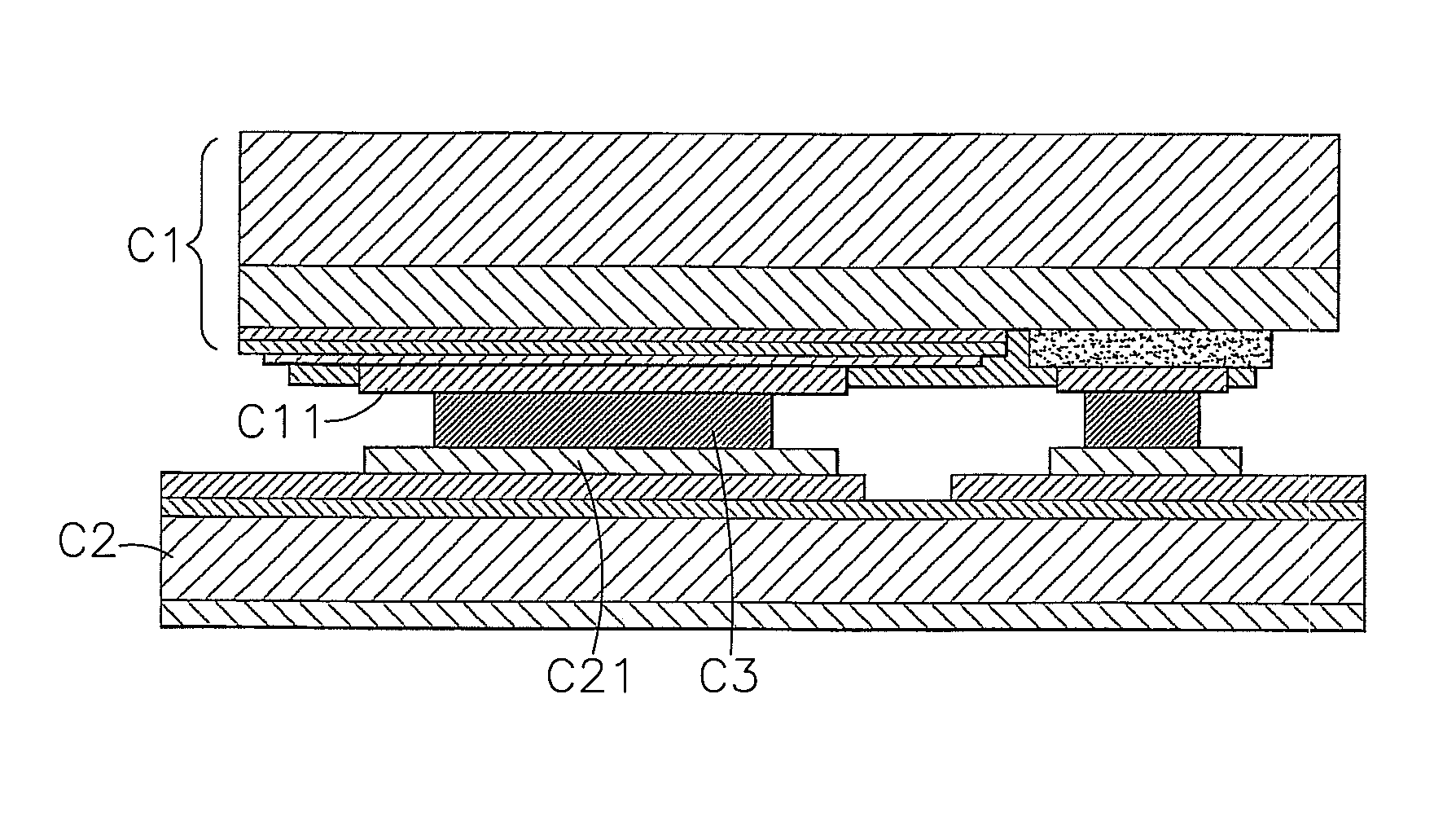
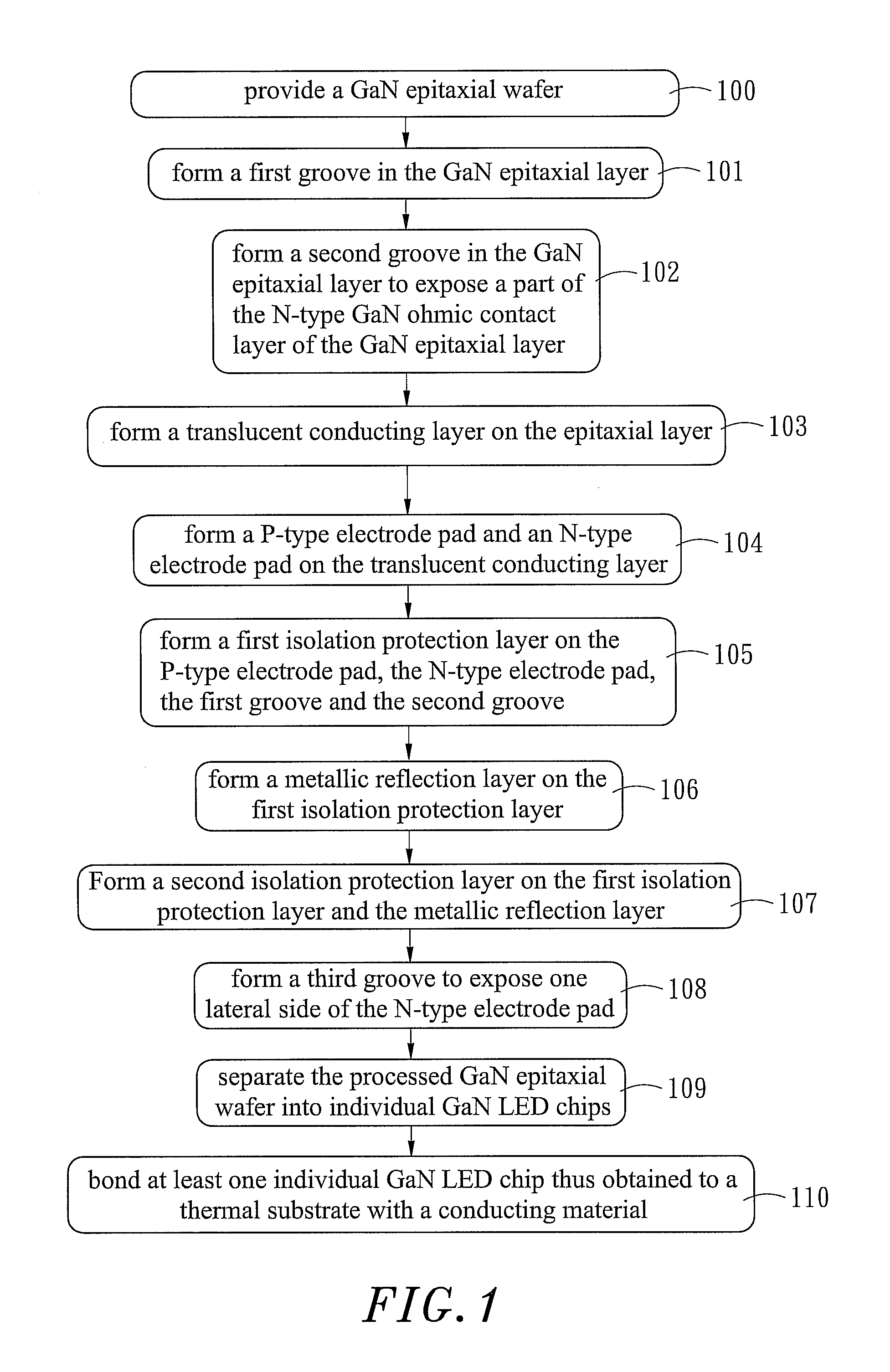
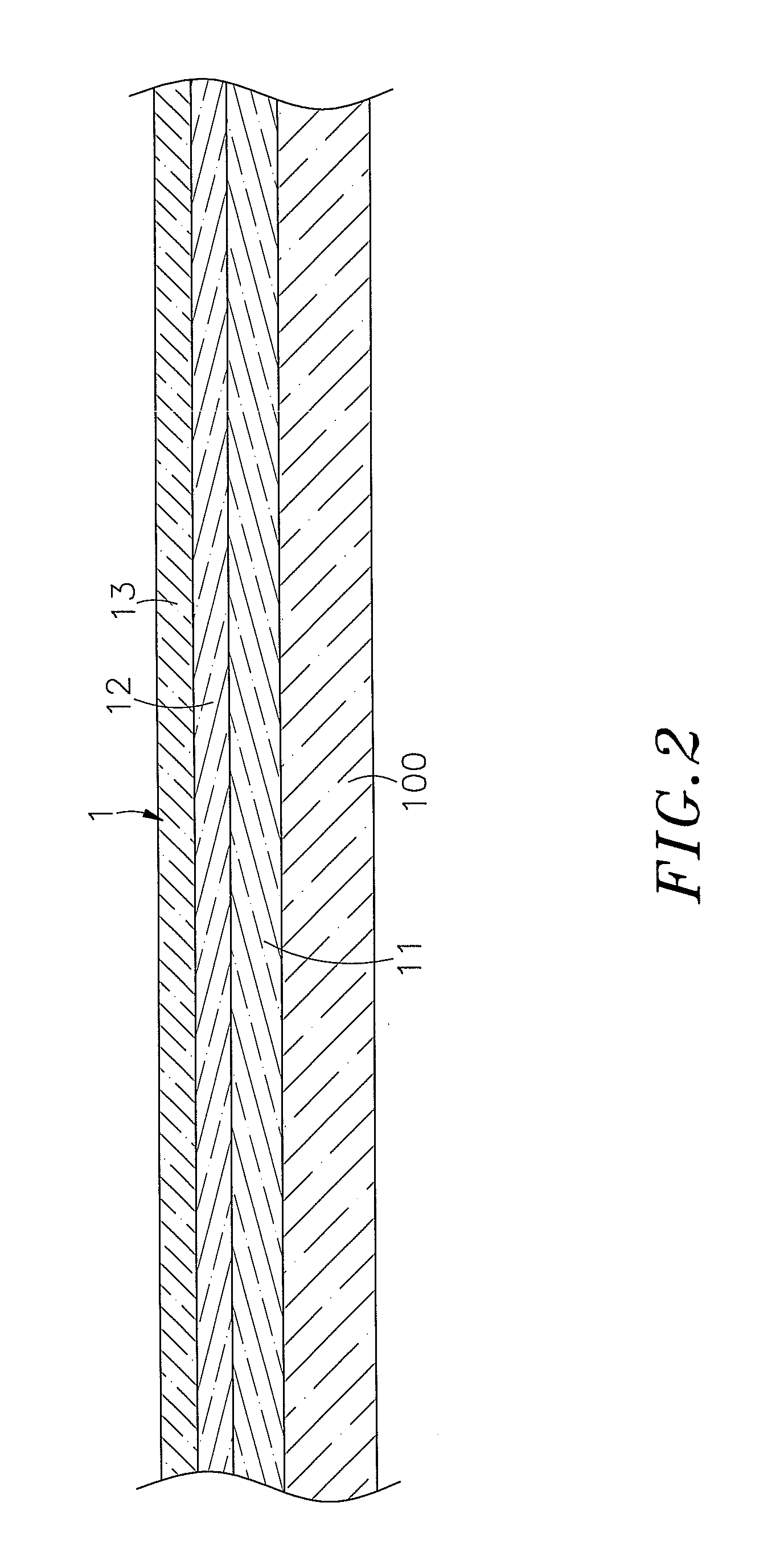
[0037]Referring to FIGS. 1˜4, a flip-chip LED fabrication method in accordance with the present invention includes the steps of:[0038](100). Provide a GaN (Gallium Nitride) epitaxial wafer consisting of a GaN epitaxial layer 2, which comprises a N-type GaN ohmic contact layer 11, a light-emitting layer 12 and a P-type semiconductor layer 13 and is arranged on a substrate 100 (see FIG. 2).[0039](101) Form a first groove 101 in the GaN epitaxial layer 2 at a predetermined location by etching to expose a part of the substrate 100 of the GaN epitaxial wafer (see FIG. 3).[0040](102) Form a second groove 102 in the GaN epitaxial layer 2 at a predetermined location adjacent to the first groove 101 by etching to expose a part of the N-type GaN ohmic contact layer 11 of the GaN epitaxial layer 2 so that the GaN epitaxial layer 2 is divided by the second groove 102 into two epitaxial layer portions 2A; 2B (see FIG. 4).[0041](103) Form a translucent conducting layer 14 on the surface of the ep...


PUM

PropertyMeasurementUnit
thicknessaaaaaaaaaa
metallicaaaaaaaaaa
etching depthaaaaaaaaaa

Abstract

A flip-chip LED fabrication method includes the steps of (a) providing a GaN epitaxial wafer, (b) forming a first groove in the GaN epitaxial layer, (c) forming a second groove in the GaN epitaxial layer to expose a part of the N-type GaN ohmic contact layer of the GaN epitaxial layer, (d) forming a translucent conducting layer on the epitaxial layer, (e) forming a P-type electrode pad and an N-type electrode pad on the translucent conducting layer, (f) forming a first isolation protection layer on the P-type electrode pad, the N-type electrode pad, the first groove and the second groove, (g) forming a metallic reflection layer on the first isolation protection layer, (h) forming a second isolation protection layer on the first isolation protection layer and the metallic reflection layer, (i) forming a third groove to expose one lateral side of the N-type electrode pad, (j) separating the processed GaN epitaxial wafer into individual GaN LED chips, and (k) bonding at least one individual GaN LED chip thus obtained to a thermal substrate with a conducting material.

Description

BACKGROUND OF THE INVENTION[0001]This application is a Continuation-In-Part of application Ser. No. 12 / 505,991, filed on Jul. 20, 2009, now pending. The patent application identified above is incorporated here by reference in its entirety to provide continuity of disclosure.[0002]1. Field of the Invention:[0003]The present invention relates to LED fabrication technology and more particularly, to a flip-chip GaN-based LED fabrication method, which enables a high reliable GaN LED chip to be bonded to a thermal substrate having a large heat dissipation area with a conducting adhesive, facilitating heat dissipation, enhancing the luminous efficiency of the GaN LED chip and prolonging its lifespan.[0004]2. Description of the Related Art:[0005]Many different types of light emitting apparatus are commercially available. Following the trend of the next generation for green energy, LED (light emitting diode), more particularly, white LED has been intensively used in street lamps, tunnel lamp...

Claims


Application Information

Patent Timeline
Patent Type & Authority Applications(United States)
IPC IPC(8): H01L33/10
CPCH01L33/20H01L33/385H01L33/44H01L33/46H01L33/62H01L33/647H01L2224/45124H01L2933/0016H01L2224/48091H01L2924/3011H01L2924/01019H01L2224/45144H01L2924/00014H01L2924/00H01L2924/00015
Inventor LU, LIEN-SHINE
Owner ENERLIGHTING CORP
Why Eureka
Try Eureka