Ion beam irradiation system and ion beam irradiation method

a technology of ion beam and ion beam, which is applied in the direction of discharge tube/lamp details, magnetic discharge control, instruments, etc., can solve the problems of unexpected in-plane non-uniform dose amount and the inability to apply the ion beam irradiation method, so as to increase the wafer productivity, and reduce the beam scan area

Active Publication Date: 2011-12-08
SENCORP
View PDF9 Cites 32 Cited by
  • Summary
  • Abstract
  • Description
  • Claims
  • Application Information

AI Technical Summary

Benefits of technology

It is an object of this invention to provide an ion beam irradiation system and an ion beam irradiation method capable of not only increasing beam irradiation efficiency but also maintaining the in-plane dose uniformity of a wafer even when small fluctuation of ion beam current happens, for an ion implanter which comprises reciprocating wafer moving function by a mechanical Y-scan device.
According to this invention, since the shape of the scan area is determined in consideration of the shape of the wafer, it is possible to reduce the beam scan area (ion beam irradiation area) with keeping the in-plane dose uniformity and to reduce the useless ion beam irradiation by reduction of ion beam quantity which is irradiated outside of the wafer, relative to the conventional rectangular beam scan area explained in FIG. 8. Thus, it is possible to reduce the amount of the ions, except for the required ion species, which are caused by the sputtering of the useless ion beam irradiation to be implanted to the wafer.

Problems solved by technology

Therefore, such an ion beam irradiation method can not be applied to an ion implanter which comprises reciprocating wafer moving function by a mechanical Y-scan device, as shown in Patent Document 1.
Further, in the ion beam irradiation method disclosed in Patent document 2, a small fluctuation of ion beam current during ion implantation to a wafer is ignored, which causes unexpected in-plane non-uniformity of the dose amount.

Method used


Image

  • Ion beam irradiation system and ion beam irradiation method
  • Ion beam irradiation system and ion beam irradiation method
  • Ion beam irradiation system and ion beam irradiation method

Examples


example

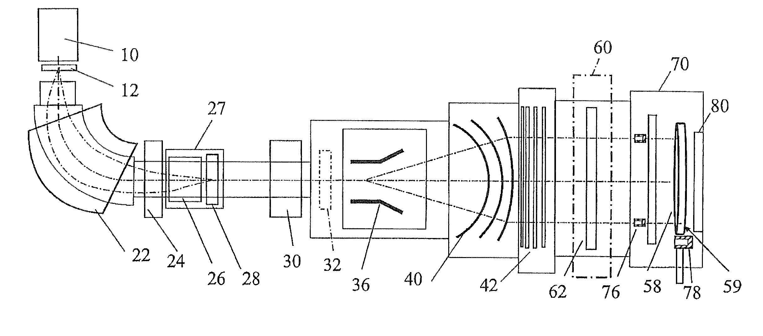
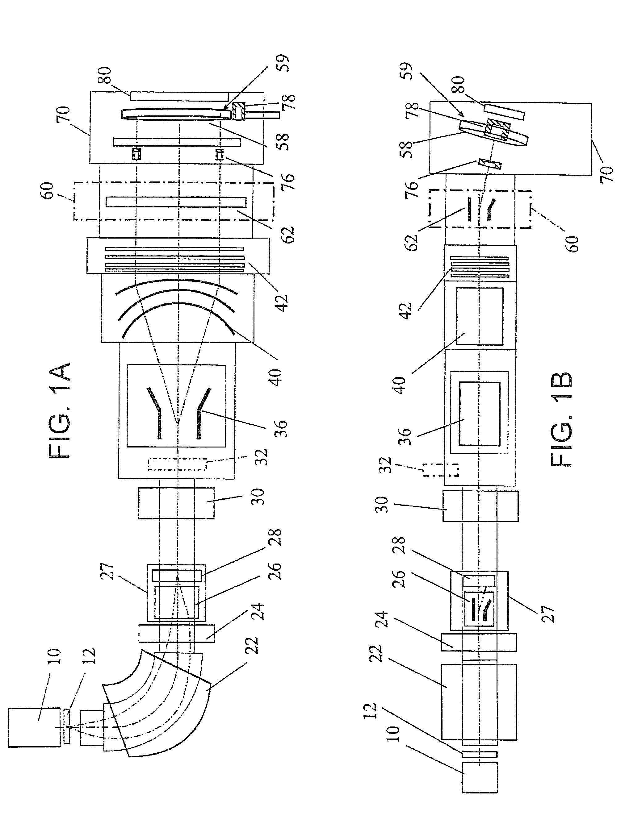
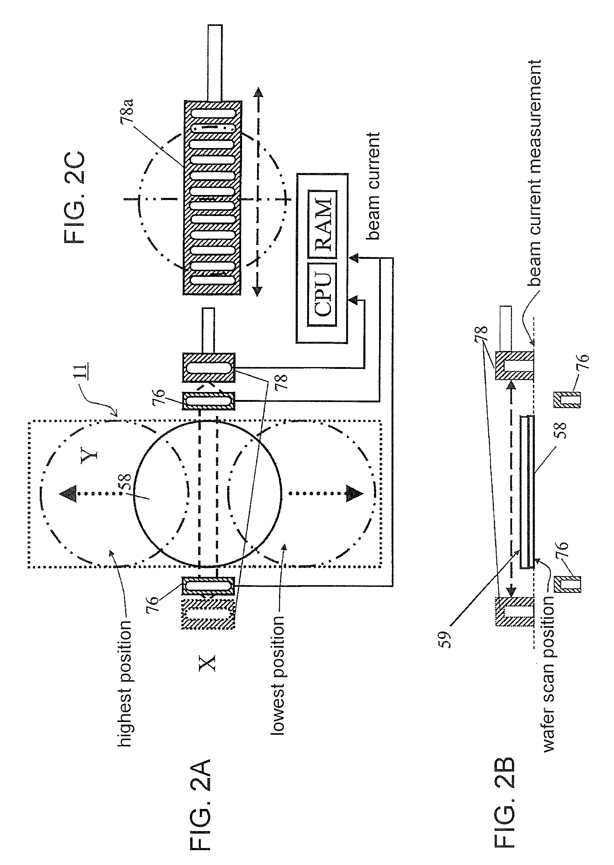
Before start of the ion implantation, the beam scan control calculation unit (CPU in FIG. 2A) 1 obtains, by calculation, the scan voltage correction function with the maximum beam scan width by using the beam measurement result according to the beam current measurement device with the maximum beam scan width. Depending on the calculated scan voltage correction function, the beam scan control calculation unit automatically calculates more than one scan voltage correction functions that realize scheduled beam scan reduction while satisfying the dose uniformity in the horizontal direction (X direction) and stores the calculated more than one scan voltage correction functions in the RAM.

The dose amount irradiated to the wafer per unit time is increased with decreasing the beam scan width, because lower beam scan speed is set.

Further, the beam scan control calculation unit controls the mechanical Y-scan speed as a function of set beam current value in order to keep (ensure) good dose uni...


PUM


Abstract

An ion beam irradiation method comprises calculating a scan voltage correction function with the maximum beam scan width depending on the measurement result of a beam current measurement device, calculating each of more than one scan voltage correction functions corresponding to each of scheduled beam scan widths depending on the calculated scan voltage correction functions while satisfying dose uniformity in the horizontal direction, measuring a mechanical Y-scan position during the ion implantation, changing the scan voltage correction function as a function of the measured mechanical Y-scan position so that the beam scan area becomes a D-shaped multistage beam scan area corresponding to an outer periphery of a half of the wafer to thereby reduce the beam scan width, and changing a mechanical Y-scan speed depending on the change of the measurement result of a side cup current measurement device to thereby keep the dose uniformity in the vertical direction.

Description

This application is based upon and claims the benefit of priority from Japanese patent application No. 2010-130378, filed on Jun. 7, 2010, the disclosure of which is incorporated herein its entirety by reference.BACKGROUND OF THE INVENTIONThis invention relates to an ion beam irradiation system and an ion beam irradiation method for use in a beam processing system using an ion beam or a charged particle beam.An ion implanter is used in order to implant ions to a circular wafer for semi-conductor device. Generally, a beam generation source, an extraction electrode, a mass analysis magnet, a mass analysis slit, an acceleration / deceleration device, and a wafer treatment chamber are aligned to a beam line in an ion implanter.Since a cross section of an ion beam is generally smaller than the size of the circular wafer, several methods have been proposed to irradiate such an ion beam to whole of the circular wafer.As one of the examples for an ion beam irradiation method, it has been prop...

Claims


Application Information

Patent Timeline
Patent Type & Authority Applications(United States)
IPC IPC(8): H01J3/26
CPCH01J37/304H01J37/3171H01J2237/31703H01J2237/30483H01J2237/24405H01J37/244H01J37/317
Inventor NINOMIYA, SHIROYUMIYAMA, TOSHIOKIMURA, YASUHIKOKUDO, TETSUYAOCHI, AKIHIRO
Owner SENCORP
Why Eureka
Try Eureka