Gallium nitride-based flip-chip light-emitting diode with double reflective layers on its side and fabrication method thereof

Inactive Publication Date: 2011-12-08
XIAMEN SANAN OPTOELECTRONICS TECH CO LTD
View PDF8 Cites 99 Cited by
  • Summary
  • Abstract
  • Description
  • Claims
  • Application Information

AI Technical Summary

Benefits of technology

[0026]The technical solution of the present invention has the advantages that: by arranging a double reflection structure including a DBR and a metal reflective layer

Problems solved by technology

However, semiconductor light sources are limited in light-emission efficiency and production cost, which makes their wide application problematic.
However, the invention uses a single metal layer as the light-emitting reflective laye

Method used


Image

  • Gallium nitride-based flip-chip light-emitting diode with double reflective layers on its side and fabrication method thereof
  • Gallium nitride-based flip-chip light-emitting diode with double reflective layers on its side and fabrication method thereof
  • Gallium nitride-based flip-chip light-emitting diode with double reflective layers on its side and fabrication method thereof

Examples


Embodiment Construction

[0029]The present invention will be further described hereinafter with reference to the embodiments and the accompanying drawings.

[0030]A fabrication method for a GaN-based flip-chip LED with double reflective layers on its side includes the following steps:

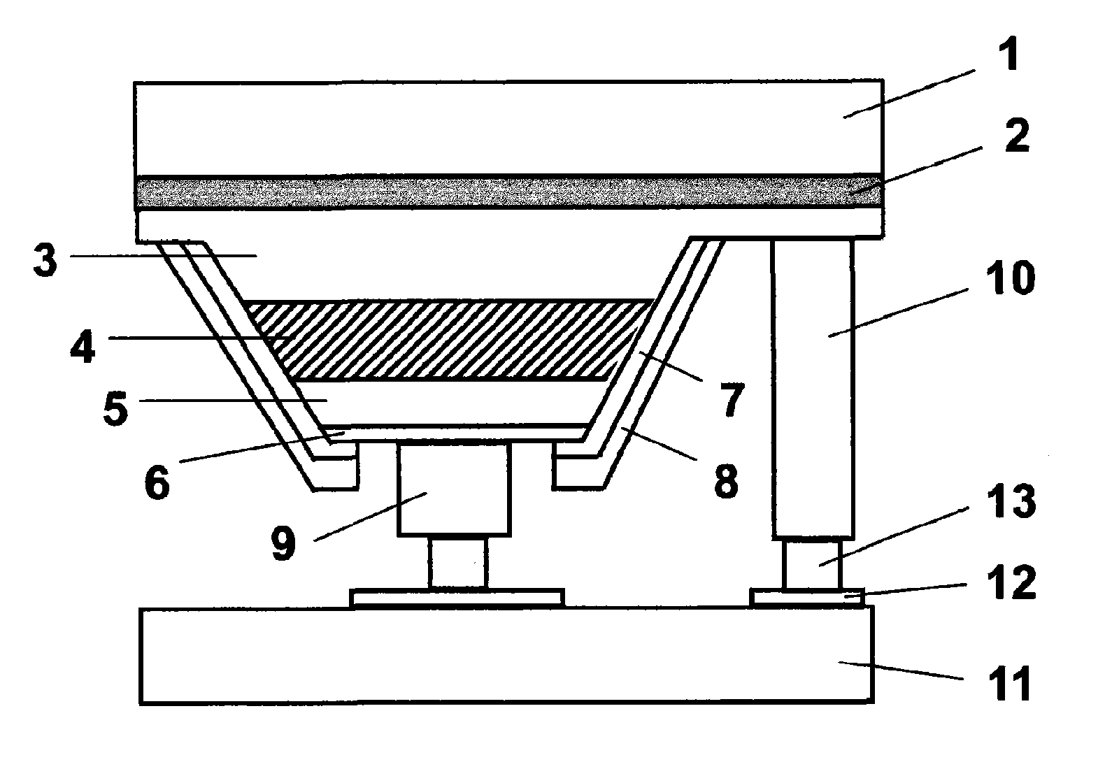
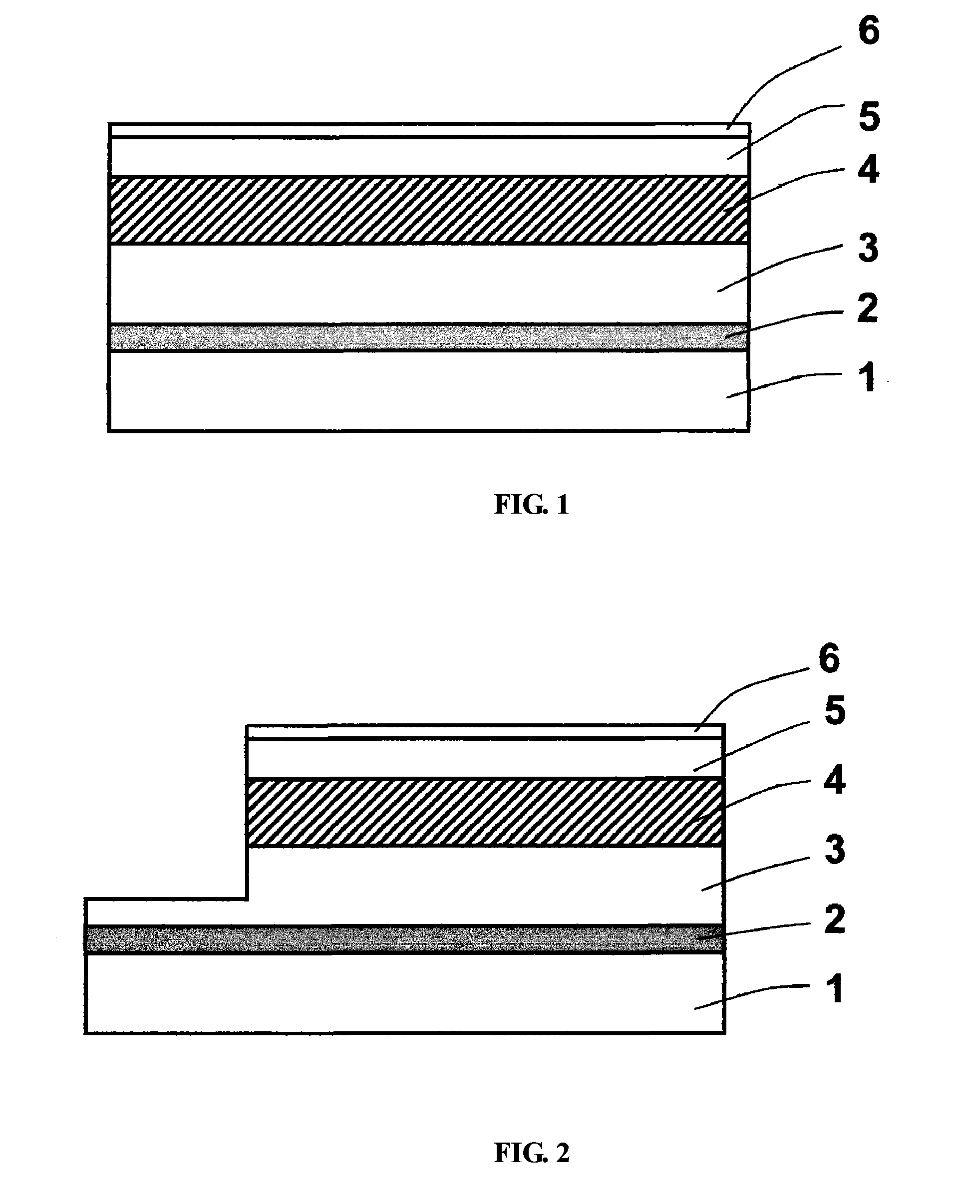
[0031]as shown in FIG. 1, forming a buffer layer 2 and an epitaxial layer on a sapphire substrate 1 in that order, with the epitaxial layer includes an N-GaN layer 3, a multiple-quantum-well layer 4 and a P-GaN layer 5; and forming an ITO transparent conductive layer 6 on the P-GaN layer 5;

[0032]as shown in FIG. 2, mask etching a portion of the mesa with the ITO transparent conductive layer 6 such that the N-GaN layer 3 is exposed;

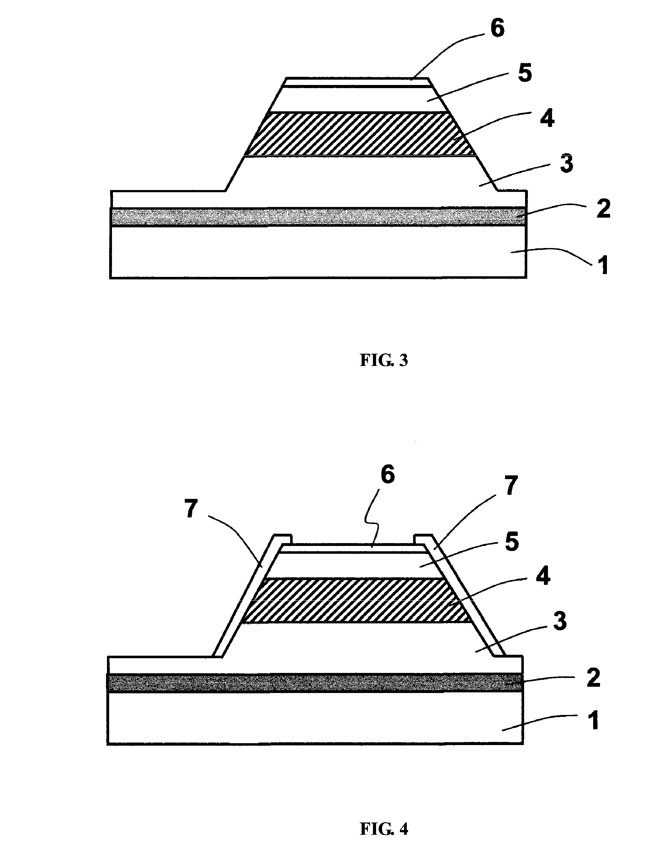
[0033]as shown in FIG. 3, cutting the epitaxial layer and the ITO transparent conductive layer 6 such that the epitaxial layer and the ITO transparent conductive layer 6 have a sloping side;

[0034]as shown in FIG. 4, forming a DBR 7 over the sloping side of the epitaxial layer and the ITO transparent con...


PUM


Abstract

The present invention discloses a double-reflective-layer gallium nitride-based flip-chip light-emitting diode with both a distributed Bragg reflector and a metal reflective layer on its side and a fabrication method thereof. The light-emitting diode includes: a sapphire substrate; a buffer layer, an N-GaN layer, a multiple-quantum-well layer and a P-GaN layer stacked on the sapphire substrate in that order; a transparent conductive layer formed on the P-GaN layer; a distributed Bragg reflector formed over a side of the epitaxial layer and the transparent conductive layer; a metal reflective layer formed on the DBR; a P-type ohmic contact electrode formed on the transparent conductive layer; and an N-type ohmic contact electrode formed on the exposed N-GaN layer, wherein the P-type ohmic contact electrode and the N-type ohmic contact electrode are bonded to a heat dissipation substrate through a metal conductive layer and a ball bonder. By arranging a double reflection structure including a DBR and a metal reflective layer on the sloping side of the LED chip, the good reflectivity of the reflective layers can be fully utilized, thereby improving the light-emission efficiency of the LED.

Description

FIELD OF THE INVENTION[0001]The present invention relates to a gallium nitride (GaN) based light-emitting diode (LED), and particularly to a GaN-based flip-chip LED with double reflective layers on its side and a fabrication method thereof.BACKGROUND OF THE INVENTION[0002]With the improvement of power GaN-based LEDs in efficiency, it is clear that GaN-based LEDs are to be a viable replacement for conventional light sources. However, semiconductor light sources are limited in light-emission efficiency and production cost, which makes their wide application problematic. Nowadays, the methods to improve the light-emission efficiency of LEDs generally include: patterned substrate, transparent substrate, Distributed Bragg Reflector (DBR) structure, surface patterning, flip-chip, chip bonding, and laser lift-off techniques. Chinese patent application 200410095820.X discloses a flip-chip light-emitting device and a method for fabricating the same. The flip-chip light-emitting device includ...

Claims


Application Information

Patent Timeline
IPC IPC(8): H01L33/06
CPCH01L33/20H01L33/46H01L33/42
Inventor ZHENG, JIANSENLIN, SUHUIHE, ANHELIN, KECHUANG
Owner XIAMEN SANAN OPTOELECTRONICS TECH CO LTD
Why Eureka
Try Eureka