Method of fabricating semiconductor device

Active Publication Date: 2011-12-08
SHARP KK
View PDF4 Cites 14 Cited by
  • Summary
  • Abstract
  • Description
  • Claims
  • Application Information

AI Technical Summary

Benefits of technology

[0029]According to the present invention, a method of fabricating a semiconductor device capable of preventing reduction in dopan

Problems solved by technology

Therefore, the method disclosed in Patent Literature 1 described above is disadvantageous in that diffusion of dopants in the back surface of the silicon substrate is not controllable since the dopants out-diffus

Method used


Image

  • Method of fabricating semiconductor device
  • Method of fabricating semiconductor device
  • Method of fabricating semiconductor device

Examples


first embodiment

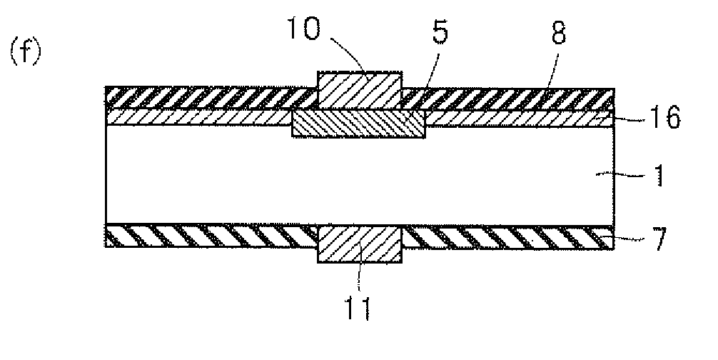
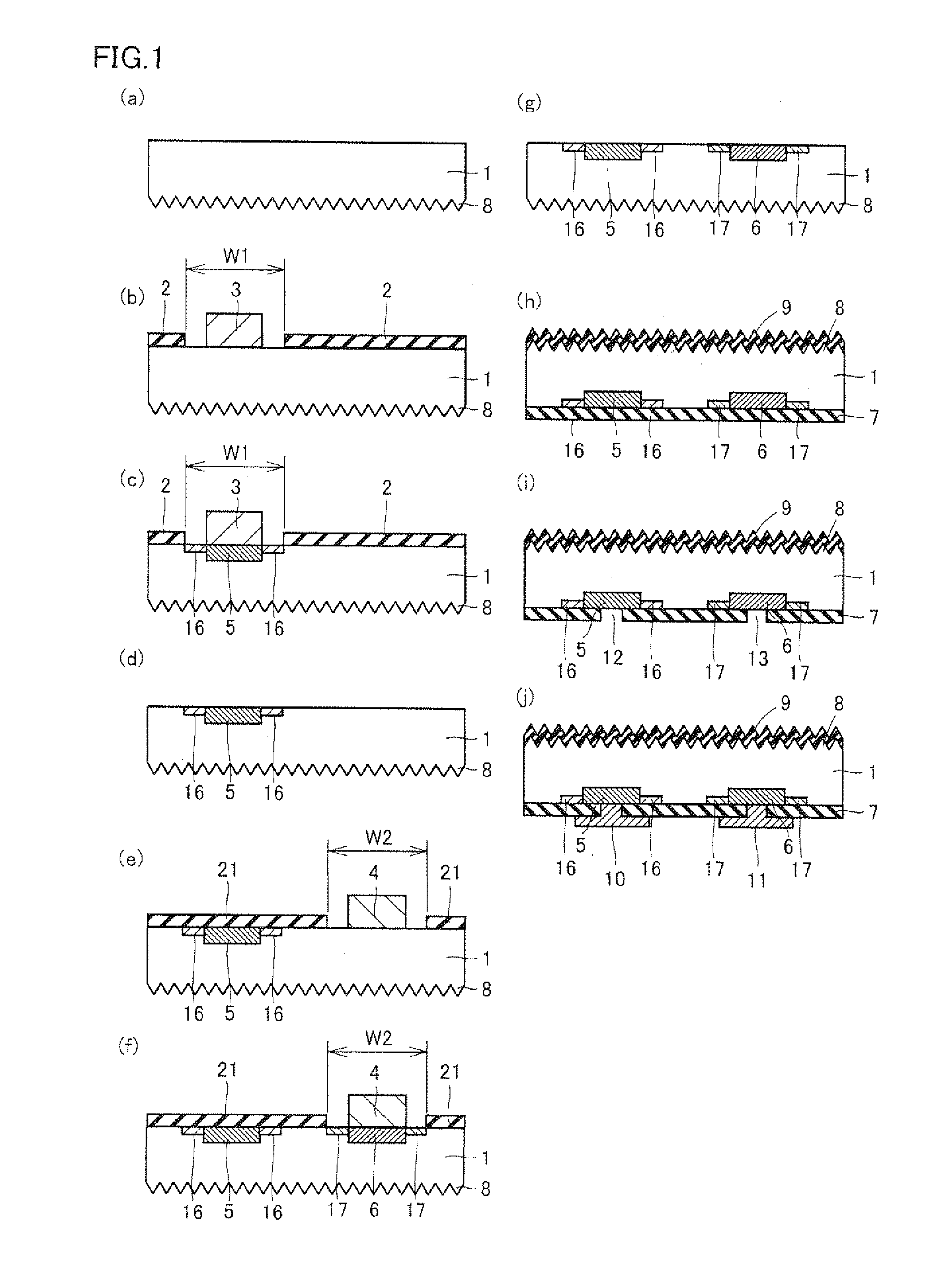
[0039]Referring to the schematic sectional views of FIG. 1(a) to FIG. 1(j), an example of a method of fabricating a solar cell which is an example of a semiconductor device according to the present invention will now be described.

[0040]First, as shown in FIG. 1(a), a semiconductor substrate 1 with a textured structure 8 made of, for example, pyramid-like irregularities or the like formed thereon is prepared. Herein, semiconductor substrate 1 is not particularly limited only if it is a substrate made of semiconductor. For example, a silicon substrate obtained by slicing a silicon ingot can be used. Moreover, semiconductor substrate 1 may be of n-conductivity type or p-conductivity type.

[0041]When using a silicon substrate as semiconductor substrate 1, a silicon substrate from which slice damage produced by slicing of a silicon ingot has been removed may be used, for example. It is noted that above-described removal of slice damage can be performed by etching the surface of the silico...

second embodiment

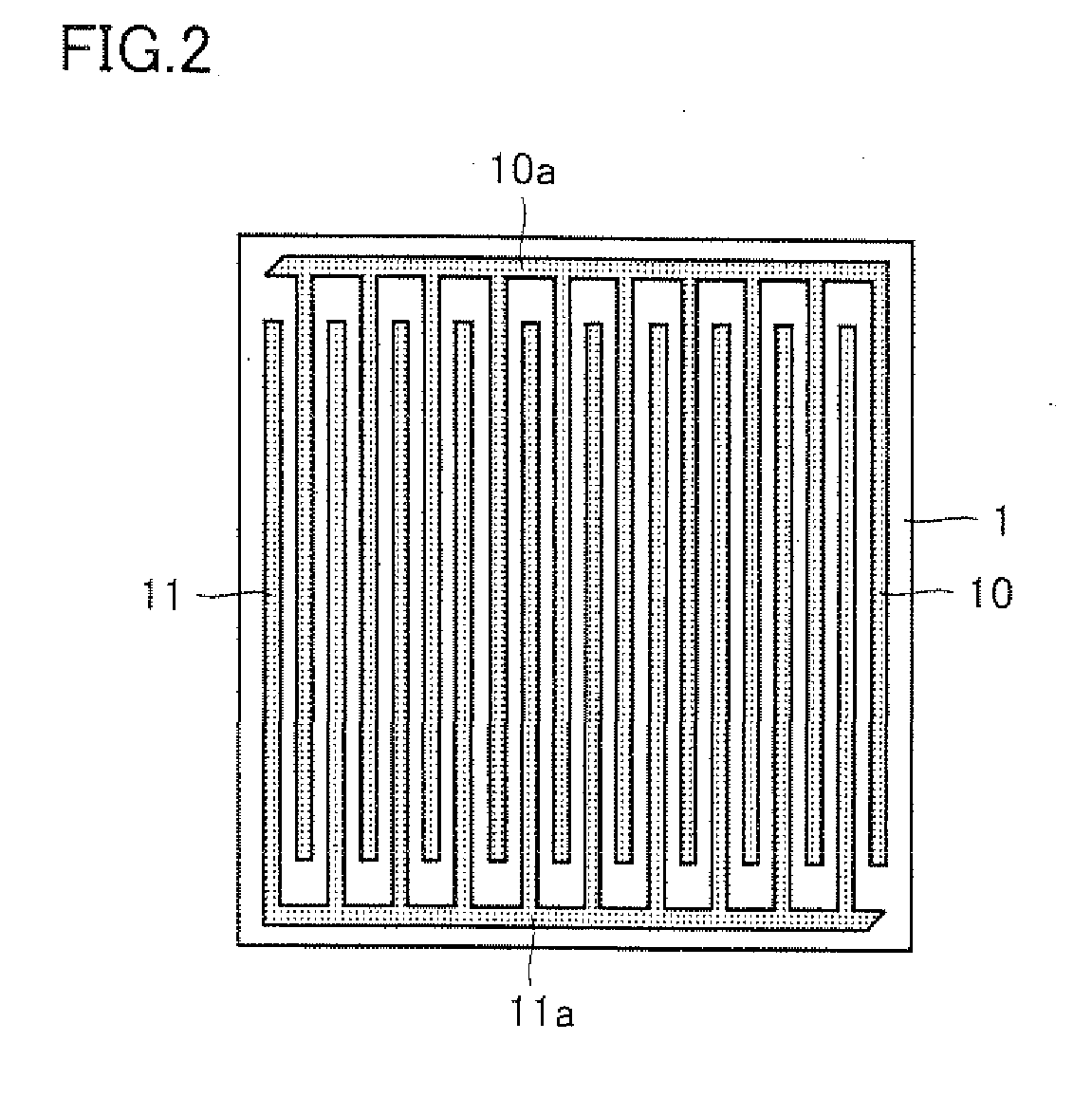
[0110]The present embodiment features applying first-conductivity-type-dopant diffusing agent 3 at an opening formed between diffusion preventing masks 2 disposed on the back surface of semiconductor substrate 1 and second-conductivity-type-dopant diffusing agent 4 at another opening formed with diffusion preventing mask 2 disposed at the back surface of semiconductor substrate 1, respectively, and then heat-treating semiconductor substrate 1, thereby simultaneously forming high-concentration first-conductivity-type-dopant diffusion layer 5, low-concentration first-conductivity-type-dopant diffusion layer 16, high-concentration second-conductivity-type-dopant diffusion layer 6, and low-concentration second-conductivity-type-dopant diffusion layer 17. The remaining points are similar to those of the first embodiment.

[0111]Referring to the schematic sectional views of FIG. 5(a) to FIG. 5(h), a method of fabricating a solar cell according to the present embodiment will now be described...

third embodiment

[0126]The present embodiment features fabricating a bifacial solar cell having electrodes at a light-receiving surface and a back surface of a semiconductor substrate, respectively, rather than a back electrode type solar cell.

[0127]Referring to the schematic sectional views of FIG. 6(a) to FIG. 6(f), the method of fabricating a solar cell according to the present embodiment will now be described.

[0128]First, as shown in FIG. 6 (a), semiconductor substrate 1 of the second conductivity type with a textured structure (not shown) made of, for example, pyramid-like irregularities or the like formed thereon is prepared.

[0129]Then, as shown in FIG. 6(b), a first-conductivity-type-dopant diffusing agent 3a containing a first-conductivity-type dopant is applied to the light-receiving surface of semiconductor substrate 1 which is the surface at the side where the textured structure is formed, and heat treatment is performed, thereby diffusing the first-conductivity-type dopant from first-con...


PUM


Abstract

Disclosed is a method of fabricating a semiconductor device, including the steps of forming a diffusion preventing mask on a surface of a semiconductor substrate, applying a dopant diffusing agent containing a dopant of a first conductivity type or a second conductivity type onto the surface of the semiconductor substrate at a spacing from the diffusion preventing mask, and forming a dopant diffusion layer by diffusing the dopant from the dopant diffusing agent into the semiconductor substrate.

Description

TECHNICAL FIELD[0001]The present invention relates to a method of fabricating a semiconductor device, and more particularly to a method of fabricating a semiconductor device capable of preventing reduction in dopant concentration in a dopant diffusion layer to prevent degradation in characteristics of the semiconductor device.BACKGROUND ART[0002]In recent years, development of clean energy is desired due to the problem of exhaustion of energy resources, the global environmental problem such as increase in CO2 in the atmosphere, and the like, and photovoltaic generation particularly utilizing solar cells among photoelectric conversion elements is being developed, practically applied, and progressed as a new energy source.[0003]A typical solar cell is a bifacial solar cell fabricated by diffusing impurities of a conductivity type opposite to that of a monocrystalline or polycrystalline silicon substrate, for example, into a light-receiving surface of the silicon substrate to form a pn...

Claims


Application Information

Patent Timeline
IPC IPC(8): H01L21/22
CPCH01L21/2254Y02E10/547H01L31/1804H01L31/061Y02P70/50
Inventor KOHIRA, MASATSUGUFUNAKOSHI, YASUSHI
Owner SHARP KK
Why Eureka
Try Eureka