Film formation method and film formation apparatus
a film formation method and film technology, applied in the direction of coatings, chemical vapor deposition coatings, capacitors, etc., can solve the problems of deterioration of dielectric characteristics and leakage current characteristics, and achieve the effect of small leakage current and high dielectric constan
- Summary
- Abstract
- Description
- Claims
- Application Information
AI Technical Summary
Benefits of technology
Problems solved by technology
Method used
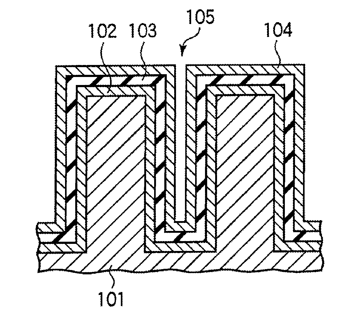
Image

Examples
Embodiment Construction
[0029]An embodiment of the present invention achieved on the basis of the findings given above will now be described with reference to the accompanying drawings. In the following description, the constituent elements having substantially the same function and arrangement are denoted by the same reference numerals, and a repetitive description will be made only when necessary.
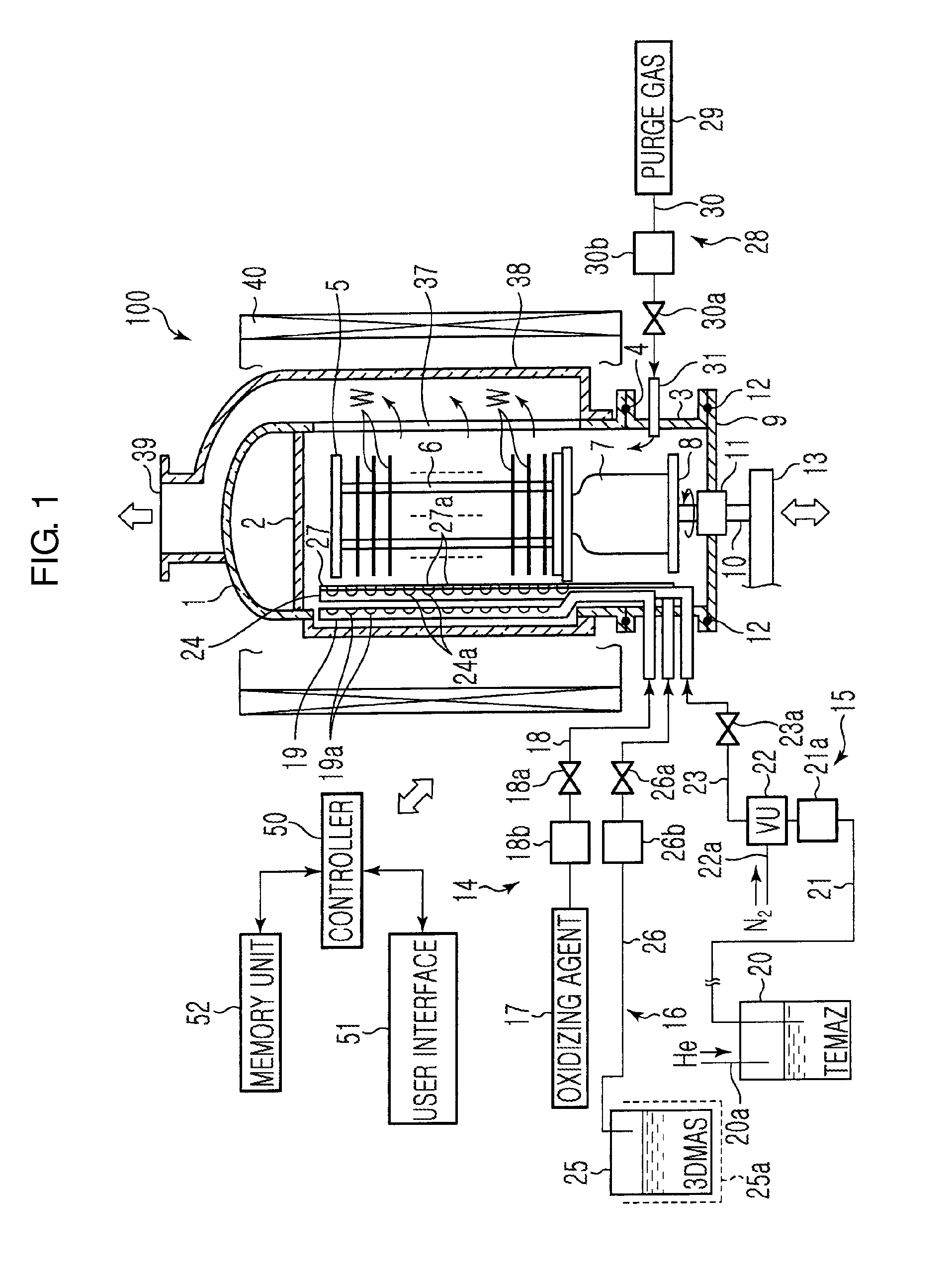
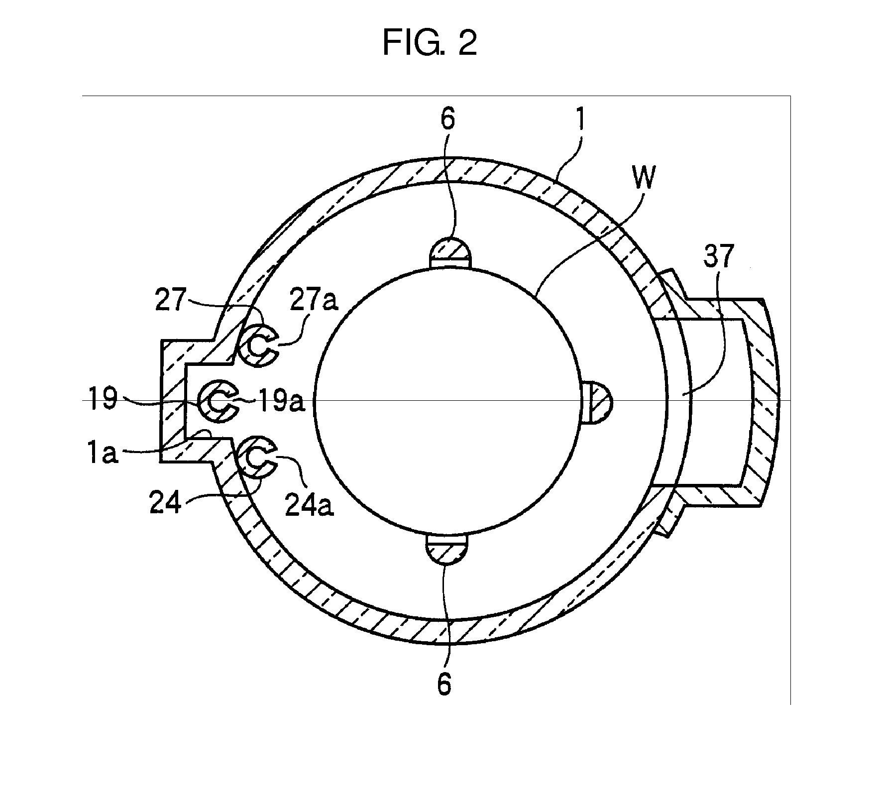
[0030]FIG. 1 is a longitudinal-sectional view showing an example of a film formation apparatus for performing a film formation method according to an embodiment of the present invention. FIG. 2 is a cross-sectional view showing the film formation apparatus of FIG. 1. FIG. 3 is a chart for explaining a film formation method according to an embodiment of the present invention. Also, in FIG. 2, a heater is not shown.
[0031]A film formation apparatus 100 includes a process chamber 1 having a shape of a bottom-open cylinder with a ceiling. The process chamber 1 is entirely formed of, for example, quartz, and a quartz ...
PUM
| Property | Measurement | Unit |
|---|---|---|
| temperature | aaaaa | aaaaa |
| dielectric constant | aaaaa | aaaaa |
| diameters | aaaaa | aaaaa |
Abstract
Description
Claims
Application Information