Ceramic electronic component and manufacturing method therefor

Active Publication Date: 2011-12-22
MURATA MFG CO LTD
View PDF8 Cites 23 Cited by
  • Summary
  • Abstract
  • Description
  • Claims
  • Application Information

AI Technical Summary

Benefits of technology

[0032]In addition, according to various preferred embodiments of the present invention, there is no need to use any water repellent agent, and the situation can be thus avoided in which the water repellent agent is applied to a location requiring plating growth.
[0033]Accordingly, preferred embodiments of the present invention allow plating growth to be easily controlled.
[0034]In addition, according to various preferred embodiments of the presen

Problems solved by technology

However, the formation of the conductive film to serve as a base leads to an increase in cost or an increase in the number of steps.
However, the condition for higher plating growth rather has difficulty with controlling plating growth, and has difficulty with placing an end edge of the plating film in a predetermined position.
Therefore, the thermistor has a problem that plating growth is likely to be caused on an undesired location of the component main body.
First, in each case of the glass layer and the water repellent layer, it is difficult to form these layers without variation in a desired location such as a location with no external terminal electrode formed, when a coating step or an immersion step is require

Method used


Image

  • Ceramic electronic component and manufacturing method therefor
  • Ceramic electronic component and manufacturing method therefor
  • Ceramic electronic component and manufacturing method therefor

Examples


Example

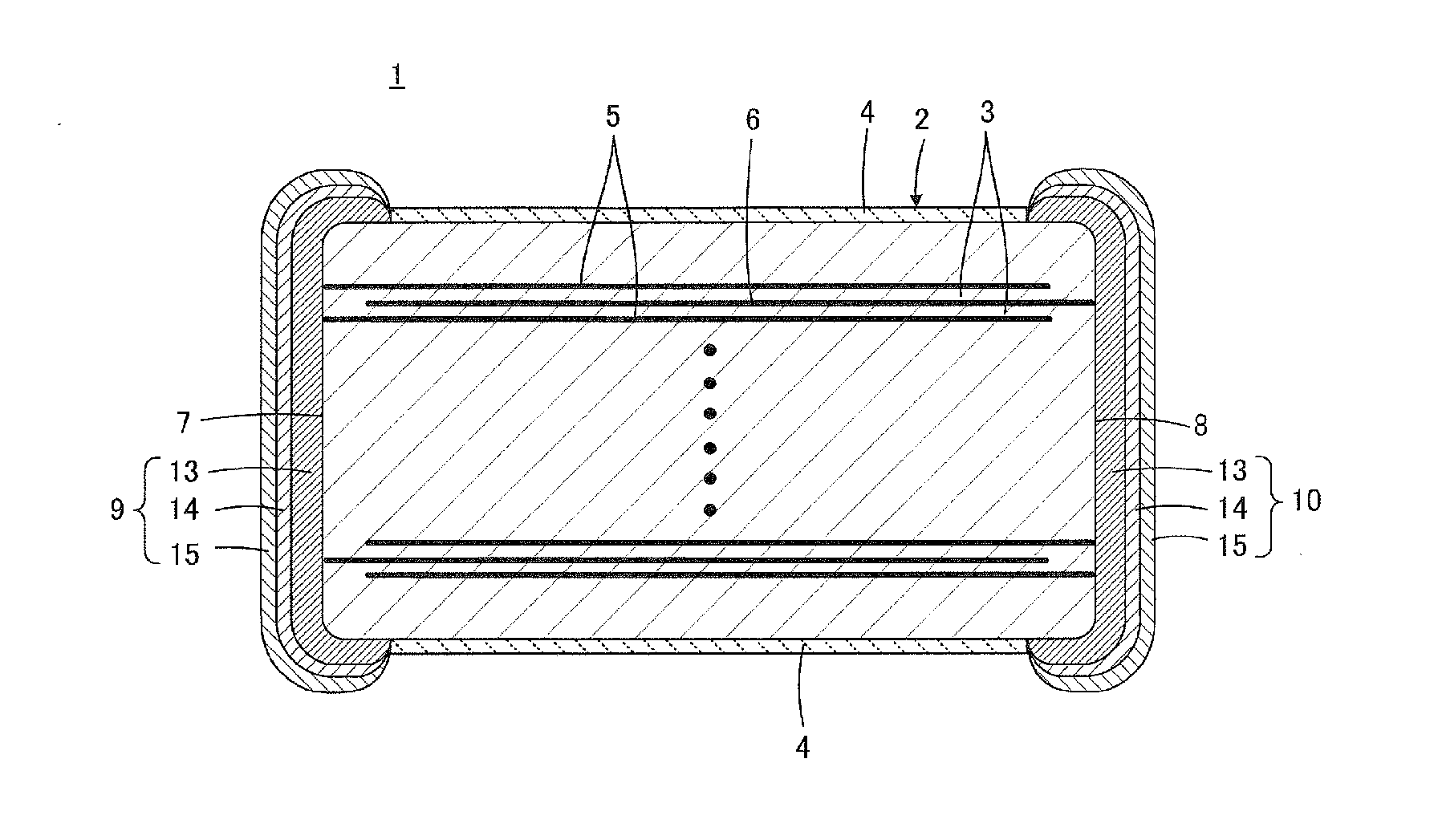
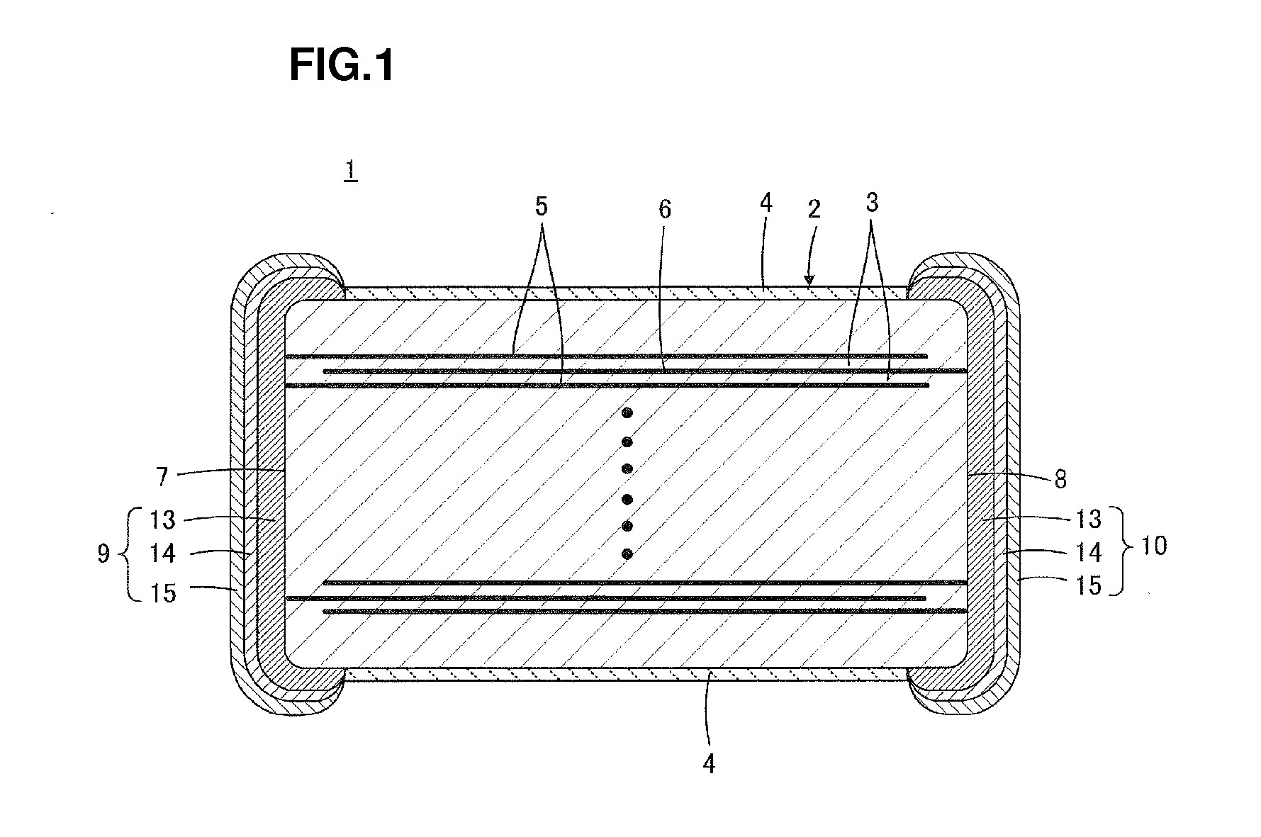
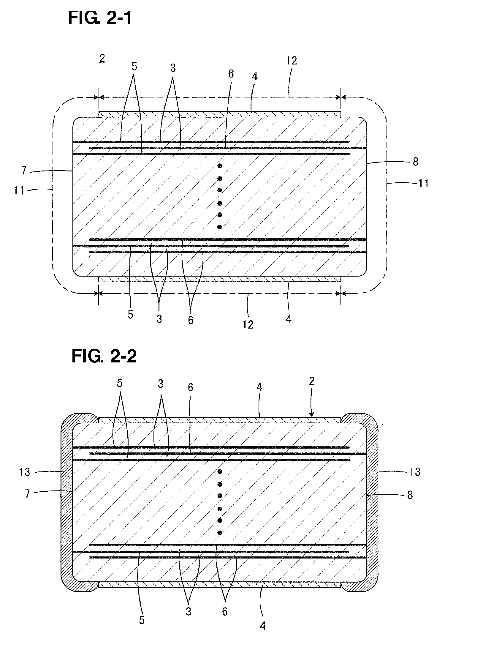
[0043]A ceramic electronic component 1 according to a preferred embodiment of the present invention will be described with reference to FIGS. 1, 2-1 and 2-2.

[0044]The ceramic electronic component 1 includes a component main body 2. The component main body 2 has a stack structure including a plurality of ceramic layers 3 and 4 stacked on each other. The ceramic layers 3 constitute intermediate layers, whereas the ceramic layers 4 constitute the outermost layers. A plurality of internal electrodes 5 and 6 are arranged along the specific interfaces between the ceramic layers 3 constituting the intermediate layers. The internal electrodes 5 and 6 preferably contain, for example, nickel as their main constituent.

[0045]The component main body 2 preferably has a rectangular parallelepiped shape or a substantially rectangular parallelepiped shape including an LW surface defined by the length dimension L and the width dimension W, an LT surface defined by the length dimension L and the thick...


PUM


Abstract

When an external terminal electrode of a ceramic electronic component such as a laminated ceramic capacitor is formed by plating, plating growth may be also caused even in an undesired location. The ceramic surface provided by a component main body is configured to include a high plating growth region of, for example, a barium titanate based ceramic, which exhibits relatively high plating growth, and a low plating growth region of, for example, a calcium zirconate based ceramic, which exhibits relatively low plating growth. The plating film constituting a first layer to define a base for an external terminal electrode is formed in such a way that the growth of a plated deposit deposited with conductive surfaces provided by exposed ends of internal electrodes as starting points is limited so as not to cross over a boundary between the high plating growth region and the low plating growth region toward the low plating growth region.

Description

BACKGROUND OF THE INVENTION[0001]1. Field of the Invention[0002]The present invention relates to a ceramic electronic component and a method for manufacturing the ceramic electronic component, and more particularly, the present invention relates to a ceramic electronic component in which an electrode such as an external terminal electrode on a component main body includes a plating film formed by plating, and a method for manufacturing the ceramic electronic component.[0003]2. Description of the Related Art[0004]As shown in FIG. 7, a laminate-type ceramic electronic component 101 typified by a laminated ceramic capacitor typically includes a component main body 105 which has a stack structure including a plurality of stacked ceramic layers 102 of, for example, a dielectric ceramic, and a plurality of layered internal electrodes 103 and 104 formed along the interfaces between the ceramic layers 102. The plurality of internal electrodes 103 and the plurality of internal electrodes 104...

Claims


Application Information

Patent Timeline
IPC IPC(8): H01L41/00H01F5/00C03B29/00H01C7/10B05D5/12H01G4/12H01C7/13H01C7/02H01C7/04H01G4/232H01G4/30
CPCH01C1/14H01G4/232H01G4/12H01G4/005
Inventor OGAWA, MAKOTOMOTOKI, AKIHIROSARUBAN, MASAHITOIWANAGA, TOSHIYUKITAKEUCHI, SYUNSUKESAKURADA, KIYOYASU
Owner MURATA MFG CO LTD
Why Eureka
Try Eureka