Supercharge Your Innovation With Domain-Expert AI Agents!

Multi-chip package semiconductor memory device

a memory device and semiconductor technology, applied in semiconductor devices, instruments, computing, etc., can solve the problems of large loss, increase in chip area, and difficulty in reducing the number of development process and manufacturing costs, so as to facilitate memory chip design and manufacture, and minimize the effect of chip area

Inactive Publication Date: 2011-12-22
LAPIS SEMICON CO LTD
View PDF20 Cites 1 Cited by
  • Summary
  • Abstract
  • Description
  • Claims
  • Application Information

AI Technical Summary

Benefits of technology

[0008]Therefore, the present invention has been made in view of the above circumstances, and it is an object of the present invention to provide an MCP type semiconductor memory device including a plurality of memory chips and having a defective cell remedy function, which enables easy design and manufacture while minimizing an increase in chip area.
[0011]The semiconductor memory device according to the present invention enables easy memory chip design and manufacture while minimizing an increase in chip area.

Problems solved by technology

If one defective cell is present in a memory chip provided in the MCP type semiconductor memory, the entire semiconductor memory becomes defective even when other memory chips are not defective, causing great loss.
That is, in this case, it is also necessary to design two types of memory chips for a single product and it is difficult to reduce the number of development processes and manufacturing costs.
However, this is undesirable since an unused function remains in the chip, causing an increase in chip area.

Method used


Image

  • Multi-chip package semiconductor memory device
  • Multi-chip package semiconductor memory device
  • Multi-chip package semiconductor memory device

Examples


embodiment 1

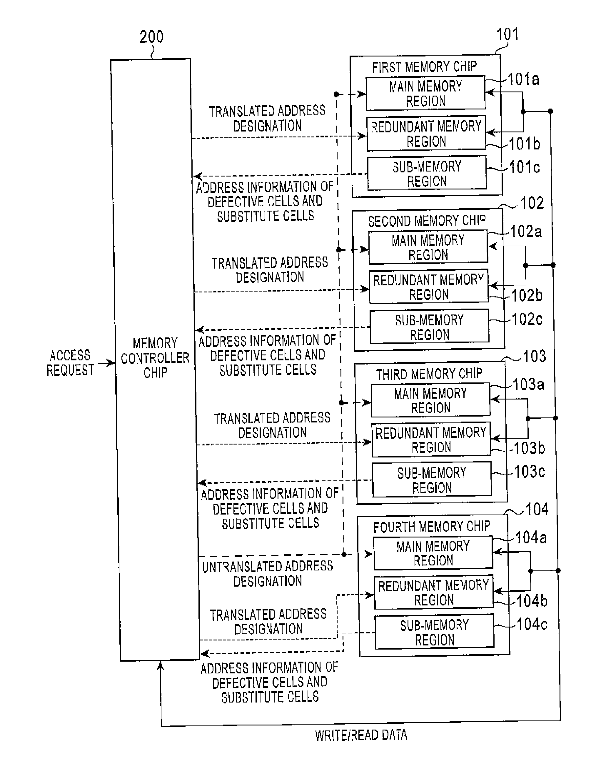
[0021]FIG. 1 is a block diagram illustrating a configuration of a semiconductor memory device 1 according to Embodiment 1 of the present invention. The semiconductor memory device 1 is an MCP type semiconductor memory device, for example, including tour memory chips 101 to 104 and a single memory controller chip 200 that are incorporated in a package.

[0022]Each of the memory chips 101 to 104 has the same circuit configuration and includes a nonvolatile storage region having a form such as, for example, a mask ROM, a Programmable ROM (PROM), an Erasable Programmable ROM (EPROM), an Electrically Erasable and Programmable ROM (EEPROM), and a flash memory. The nonvolatile storage region includes, for example, MOS-structured memory cells having floating gates. The storage regions of the memory chips 101 to 104 include main memory regions 101a to 104a, redundant memory regions 101b to 104b, and sub-memory regions 101c to 104c, respectively.

[0023]Each of the main memory regions (first stor...

embodiment 2

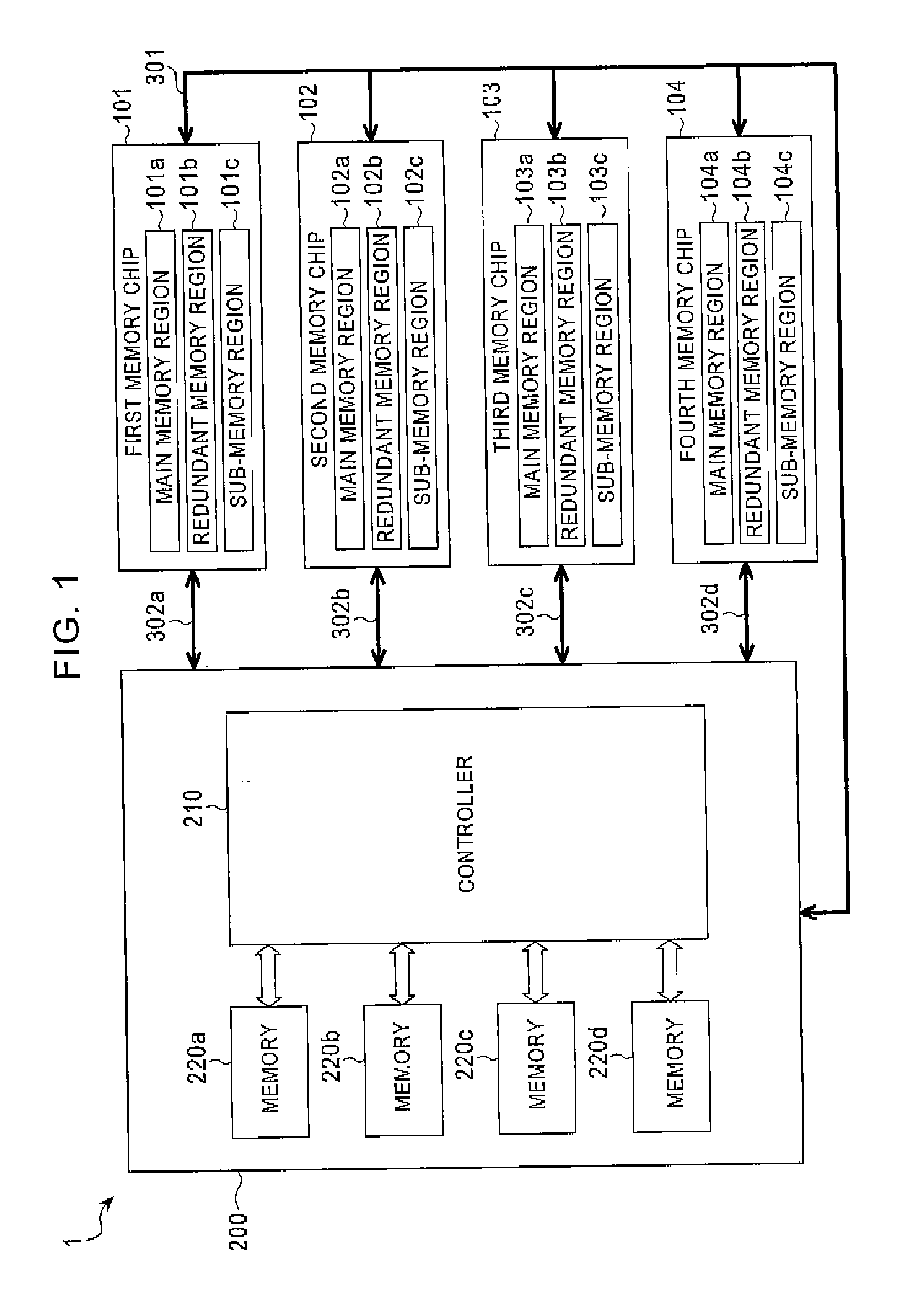
[0054]A semiconductor memory device according to Embodiment 2 of the present invention is described below. FIG. 6 is a block diagram illustrating a configuration of a semiconductor memory device 2 according to Embodiment 2 of the present invention. Similar to Embodiment 1, the semiconductor memory device 2 is an MCP type semiconductor memory device including a plurality of memory chips 105 to 108 and one memory controller chip 200 that are incorporated in a package. Internal configurations of the memory chips of the semiconductor memory device 2 are different from those of Embodiment 1. The memory chips 105 to 108 include fuse circuits 105d to 108d, which are generally used as means for remedying defective cells, in addition to main memory regions 105a to 108a, first redundant memory regions 105b1 to 108b1, second redundant memory regions 105b2 to 108b2, and sub-memory regions 105c to 108c, respectively. Each of the fuse circuits 105d to 108d includes a plurality of fuse elements co...


PUM


Abstract

An MCP type semiconductor memory device having a defective cell remedy function, which enables easy design and manufacture while minimizing chip area increase, is provided. The semiconductor memory device includes memory chips and a memory controller chip that designates an address of a memory chip according to an access request received from outside and controls access to the designated address. Each memory chip includes first and second storage regions and an information holder that holds address information representing associations between addresses in the first and second storage regions. The memory controller chip includes an address translating part that performs, upon receiving a request to access a specific address in the first storage region indicated by the address information, address designation by translating the specific address in the first storage region to an address in the second storage region corresponding to the specific address based on the associations represented by the address information.

Description

BACKGROUND OF THE INVENTION[0001]1. Field of the Invention[0002]The present invention relates to a semiconductor memory device, and more particularly to a Multi-Chip Package (MCP) type semiconductor memory device including a plurality of memory chips and one memory controller chip which are provided in one package.[0003]2. Description of the Related Art[0004]In the field of mobile devices such as mobile phones, advanced functions, such as functions to store and reproduce still images, moving images, and music, and a game function, have been increasingly adopted and there has also been a great demand for high speed processing of a large amount of data. Thus, there is a need to increase storage capacity while achieving a reduction in the size of the semiconductor memory. MCP, which incorporates a plurality of memory chips into one package, is a package technology developed to meet such a need. Particularly, a stack MCP including a stack of two or more chips is effective in reducing pa...

Claims


Application Information

Patent Timeline
Patent Type & Authority Applications(United States)
IPC IPC(8): G06F12/00
CPCG11C29/76G11C29/70H01L2224/48147
Inventor MIYAZAKI, SATOSHINASU, HIDEKAZU
Owner LAPIS SEMICON CO LTD
Features
  • R&D
  • Intellectual Property
  • Life Sciences
  • Materials
  • Tech Scout
  • Unparalleled Data Quality
  • Higher Quality Content
  • 60% Fewer Hallucinations
Learn More