


Quick Research
Generate reliable direction feasibility study reports for your R&D in just a few steps.

Technical Q&A
Discover and master advanced knowledge NOW. Basics, ideas, possibilities, all at once.

Find Solutions
As an expert in R&D theories, this can generate solutions to your technical problems instantly.

Evaluate Feasibility
Analyze your overall solution with one click, know your potential R&D risks in advance.

Monitor Landscape
Get weekly tech updates, stay abreast of the latest tech innovations and key insights.
Method for manufacturing trench type superjunction device and trench type superjunction device
- Summary
- Abstract
- Description
- Claims
- Application Information
AI Technical Summary
Benefits of technology
Problems solved by technology
Method used
Image

Examples
first embodiment
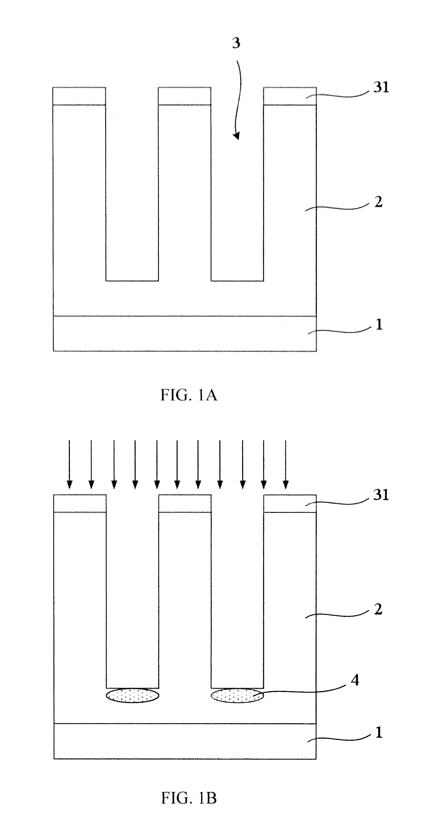
[0022]Please refer to FIGS. 1A˜1C, the method for manufacturing trench type super junction device according to the present invention includes the following steps:
[0023]Step 1, as shown in FIG. 1A, firstly form an N− epitaxial layer 2 on an N+ silicon substrate 1, wherein the Rs (Resistivity) of the N+ substrate 1 is in a range of 0.001˜0.003 Ω·cm; the thickness and the Rs of the N− epitaxial layer 2 are determined according to the design requirement of the device. For a device of 600V BVDS (breakdown voltage), the Rs of the N− epitaxial layer 2 is 2˜10 Ω·cm, and the thickness of the N− epitaxial layer 2 is 40˜55 μm.
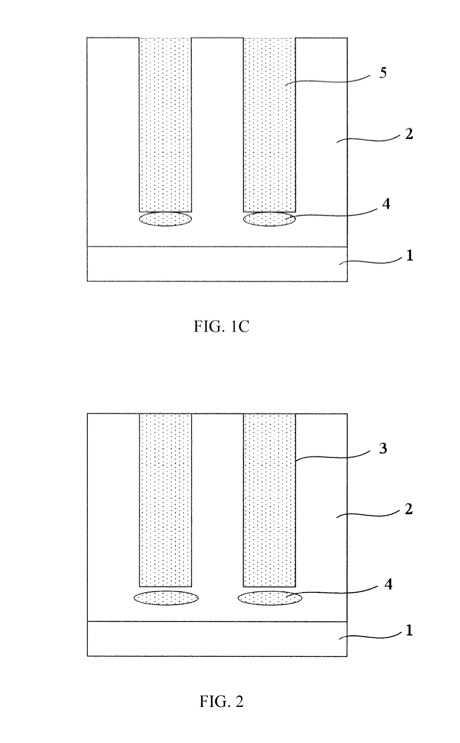
[0024]Then form a dielectric film 31 on the N− epitaxial layer 2, wherein the dielectric film 31 can be a silicon oxide film, and the dielectric film 31 can be used as hard mask during the subsequent process of trench etching and can also be used as stop layer during the subsequent process of chemical mechanical polishing.
[0025]Afterwards, form one or more trenches 3 in t...
fourth embodiment
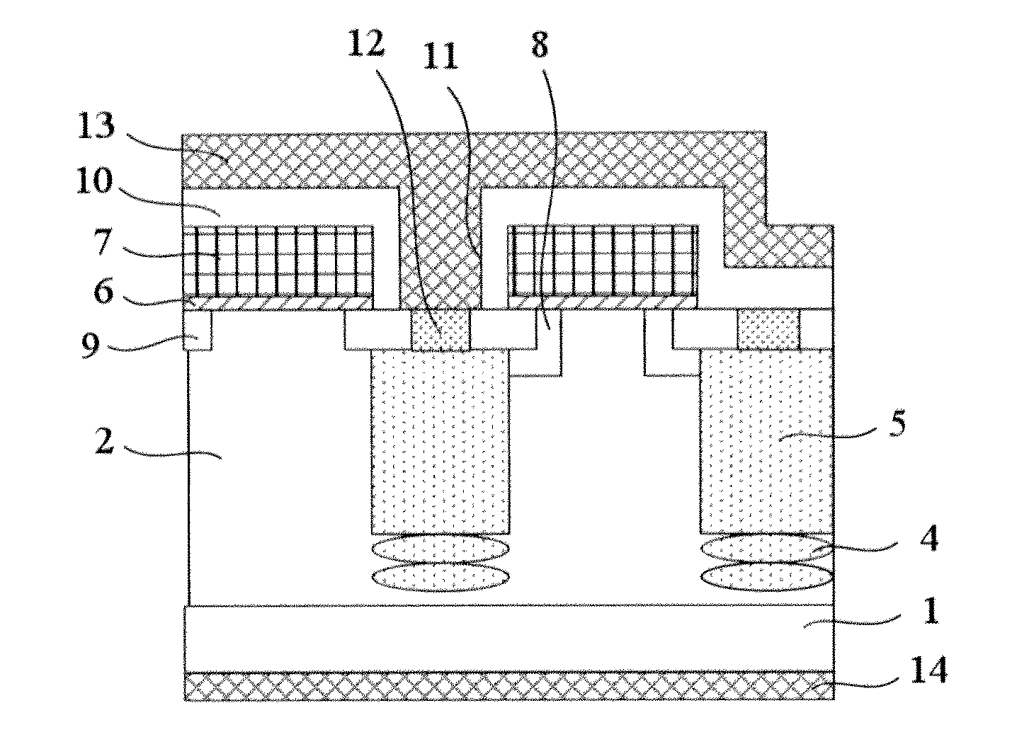
[0032]FIG. 4 shows a schematic view of the impurities implanted below the bottom of the trenches according to the present invention. In FIG. 4, more than one P type implantation regions 4 are formed below the bottom of each trench 3; the P type implantation regions 4 are not connected with one another, and the P type implantation region closest to the trench is not connected with the bottom of the trench 3. The structure as shown in FIG. 4 can be formed by performing multiple steps of P type ion implantation with different implant energies. The implant energies are controlled such that the P type implantation regions 4 below each trench are not consecutive in the vertical direction.
[0033]In other embodiments, the one or more P type implantation regions 4 below each trench 3 (either consecutive or not) may connect or disconnect with the bottom of the trench 3, and may connect or disconnect with the N+ substrate 1. There is no limit to the distribution of P type impurities. As long as...
PUM
 Abstract
Description
Claims
Application Information
 - R&D Engineer
- R&D Manager
- IP Professional
- Industry Leading Data Capabilities
- Powerful AI technology
- Patent DNA Extraction
Browse by: Latest US Patents, China's latest patents, Technical Efficacy Thesaurus, Application Domain, Technology Topic, Popular Technical Reports.
© 2024 PatSnap. All rights reserved.Legal|Privacy policy|Modern Slavery Act Transparency Statement|Sitemap|About US| Contact US: help@patsnap.com