Check patentability & draft patents in minutes with Patsnap Eureka AI!

Non-volatile storage device

a storage device and non-volatile technology, applied in static storage, digital storage, instruments, etc., can solve the problems of internal voltage csv not always matching the reference level, and achieve the effect of reducing the access delay

Active Publication Date: 2011-12-29
LAPIS SEMICON CO LTD
View PDF7 Cites 1 Cited by
  • Summary
  • Abstract
  • Description
  • Claims
  • Application Information

AI Technical Summary

Benefits of technology

[0009]In consideration of the above circumstances, an object of the present invention is to provide a non-volatile storage device enabling access delay to be further reduced.
[0018]According to the first aspect of the present invention, the bit line connected to the memory cell subject to reading is charged to the reference level in preparation to comparing the voltage level of the bit line connected to the memory cell subject to reading against the reference level, enabling the access delay to be reduced.
[0031]The non-volatile storage device of the present invention exhibits the excellent effect of enabling the access delay to be reduced.

Problems solved by technology

The voltage level of the bit line changes according to the data stored in the memory cell subject to reading, however when, say, reading data “0” after reading data “1”, it takes some time until the bit line is charged and achieves a stable state capable of determining a 0 read, causing access delay.
However, the internal voltage CSV does not always match the reference level.

Method used


Image

  • Non-volatile storage device
  • Non-volatile storage device
  • Non-volatile storage device

Examples


first exemplary embodiment

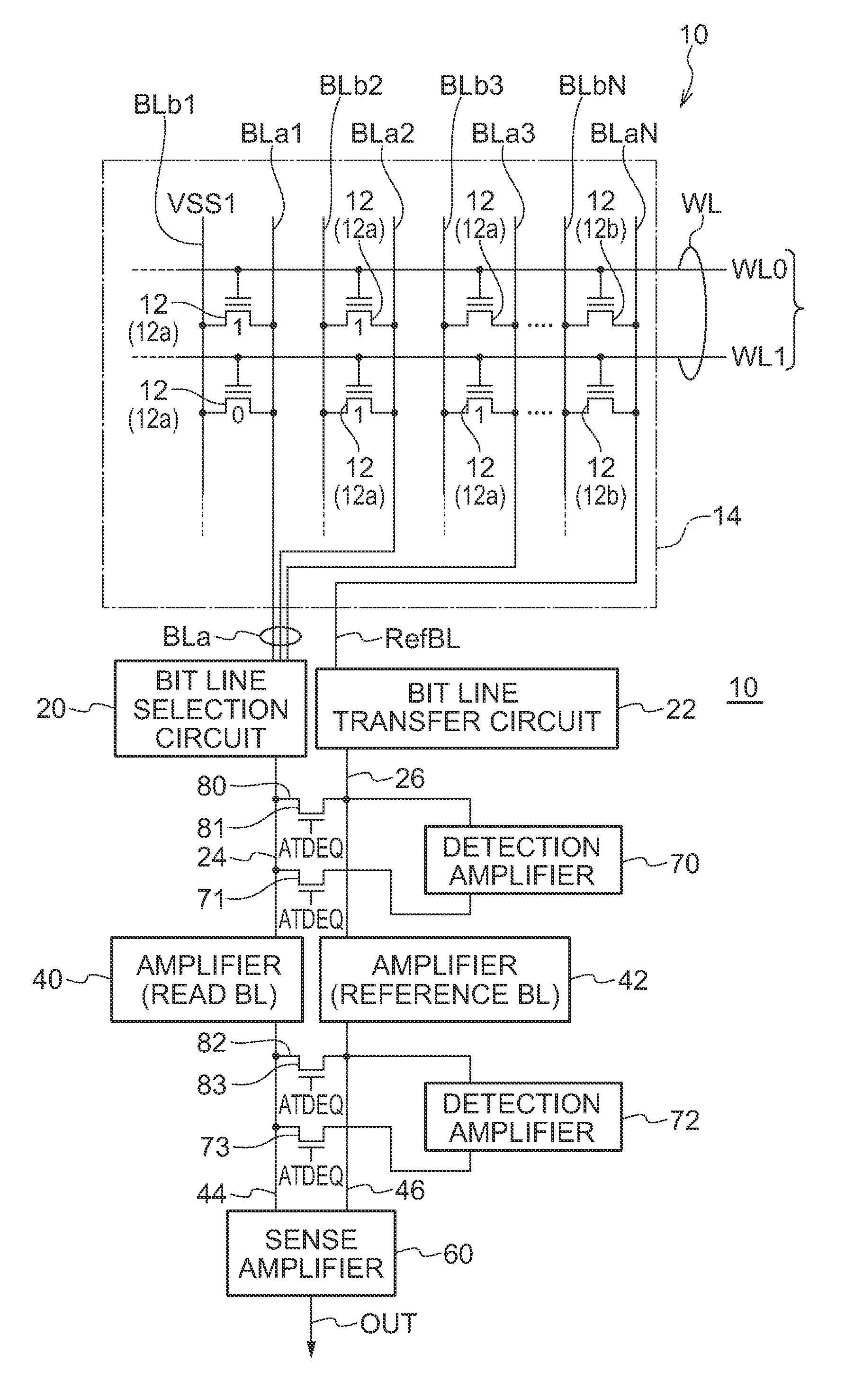
[0044]FIG. 1 is a block diagram of a non-volatile memory 10 to which the present invention is applied. Note that in the following explanation portions that are not directly related to the present invention are abbreviated in the drawing and explanation.

[0045]As shown in FIG. 1, the non-volatile memory 10 of the first exemplary embodiment includes a memory cell array 14 provided plural memory cells 12 for storing data laid out in a matrix.

[0046]The memory cell array 14 has plural word lines WL (WL0, WL1 and so on) decoded by a given external address input and disposed parallel to each other. The memory cell array 14 also has plural first bit lines BLa (BLa0, BLa1 to BLaN) for data transmission disposed parallel to each other at a specific separation interval along a direction orthogonal to the plural word lines WL. Plural second bit lines BLb (BLb0, BLb1 to BLbN) for electrical potential lowering are provided parallel to and in the vicinity of each of the respective first bit lines B...

second exemplary embodiment

[0072]Explanation now follows regarding a second exemplary embodiment.

[0073]FIG. 7 is a block diagram of a non-volatile memory 10 according to the second exemplary embodiment. Portions similar to those of the first exemplary embodiment (see FIG. 1) are allocated the same reference numerals and further explanation thereof is omitted.

[0074]In the non-volatile memory 10 of the present exemplary embodiment, the connection line 24 and the connection line 26 are connected together by a connection line 80 through a transistor 81, and the connection line 44 and the connection line 46 are connected together by a connection line 82 (serving as a connection portion) through a transistor 83.

[0075]The signal ATDEQ is input to the gates of the transistors 81, 83, and the transistors 81, 83 are turned on or off according to the signal ATDEQ.

[0076]Explanation now follows regarding operation of the non-volatile memory 10 according to the second exemplary embodiment.

[0077]In the non-volatile memory 1...


PUM


Abstract

There is provided a non-volatile storage device including: a memory array section arrayed with plural non-volatile memory cells for electronically writable data storage; plural bit lines that are connected to respective memory cells and have voltage levels that change according to the data stored in the memory cells; a supply section that supplies a voltage of a reference level to act as a comparator reference when determining data stored in the memory cells; a comparator section that compares the voltage level of the bit line connected to the memory cell subject to reading against the reference level supplied by the supply section; and a charging section that, in preparation for comparison by the comparator section, charges the bit line connected to the memory cell subject to reading to the voltage of the reference level supplied by the supply section.

Description

CROSS-REFERENCE TO RELATED APPLICATION[0001]This application is based on and claims priority under 35 USC 119 from Japanese Patent Application No. 2010-143147 filed on Jun. 23, 2010, the disclosure of which is incorporated by reference herein.BACKGROUND[0002]1. Technical Field[0003]The present invention relates to a non-volatile storage device with electronic writing capability.[0004]2. Related Art[0005]A non-volatile memory is traditionally formed, for example, with a memory array of plural memory cells respectively arrayed in word lines (WL) and bit lines (BL). The bit lines of the memory cell subject to reading are sequentially connected to a read amplifier through a selection circuit, and data is read out by comparing the voltage level of the bit line connected to the memory cell by the read amplifier against a reference level.[0006]Each of the memory cells is stored with data of “1” or “0”. The voltage level of the bit line changes according to the data stored in the memory cel...

Claims


Application Information

Patent Timeline
Patent Type & Authority Applications(United States)
IPC IPC(8): G11C7/06
CPCG11C7/1042G11C16/28G11C7/14G11C7/12
Inventor KURAMORI, BUNSHO
Owner LAPIS SEMICON CO LTD
Features
  • R&D
  • Intellectual Property
  • Life Sciences
  • Materials
  • Tech Scout
  • Unparalleled Data Quality
  • Higher Quality Content
  • 60% Fewer Hallucinations
Learn More