
Polymeric Barrier Removal Polishing Slurry

a technology of polymer barrier and polishing slurry, which is applied in the direction of electrical equipment, chemistry apparatus and processes, other chemical processes, etc., can solve the problems of new challenges for the integration of conventional chemical mechanical polishing (cmp) processes, and increasing the workload of polishing slurry for low k films

Inactive Publication Date: 2011-12-29
ROHM & HAAS ELECTRONICS MATERIALS CMP HLDG INC
View PDF3 Cites 11 Cited by
  • Summary
  • Abstract
  • Description
  • Claims
  • Application Information

AI Technical Summary

Benefits of technology

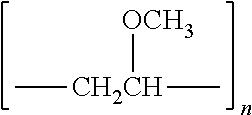
[0005]An aspect of the invention provides a aqueous slurry useful for chemical mechanical polishing a semiconductor substrate having copper interconnects comprising by weight percent, 0 to 25 oxidizing agent, 0.1 to 50 abrasive particles, 0.001 to 10 inhibitor for decreasing static etch of the copper interconnects, 0.001 to 5 poly(methyl vinyl ether) having a formula as follows:
[0006]Another aspect of the invention provides an aqueous slurry useful for chemical mechanical polishing a semiconductor substrate having copper interconnects comprising by weight percent, 0 to 20 oxidizing agent, 0.5 to 50 abrasive particles, 0.005 to 10 inhibitor for decreasing static etch of the copper interconnects, 0.005 to 5 poly(methyl vinyl ether) having a formula as follows:
[0007]Another aspect of the invention provides a method of polishing a semiconductor substrate, the semiconductor substrate having a copper layer, a TEOS layer and a low k dielectric layer, the method including the steps of: introducing polishing slurry onto a polishing pad, the polishing slurry having the composition comprising by weight percent, 0 to 25 oxidizing agent, 0.1 to 50 abrasive particles, 0.001 to 10 inhibitor for decreasing static etch of the copper interconnects, 0.001 to 5 poly (methyl vinyl ether) having a formula as follows:

Problems solved by technology

As ultra-large-scale-integrated circuit (ULSI) technology migrates to smaller lines widths, there are new challenges for the integration of conventional chemical mechanical polishing (CMP) processes.
In addition, the introduction of low k and ultra-low k dielectric films requires the use of a gentler CMP processes due to the films' low mechanical strength and weak adhesion to adjacent layers.
Furthermore, ever-tightening defectivity specifications have placed additional demands on polishing slurries for low k films.
The complexities surrounding implementation of low k materials have introduced larger challenges for the barrier CMP process, which will necessitate the ability to control the complicated input variables and achieve a consistent high yield.
Unfortunately, these slurries have inadequate barrier removal rate for some applications.

Method used


Image

  • Polymeric Barrier Removal Polishing Slurry
  • Polymeric Barrier Removal Polishing Slurry
  • Polymeric Barrier Removal Polishing Slurry

Examples


example 1

[0034]An initial series of slurries varied BTA, poly(methyl vinyl ether), potassium phosphate and aminobutyric acid to determine polishing characteristics. Polishing data are below in Table 2.

TABLE 2CuNon-TEOSCDOCuUniformitySlurry(Å / min)(Å / min)(Å / min)(%)Ta164137129114.8High264335334412.1High36292783607.6High46663604115.6High568232637111.5High673153043311.5High76793884356.1High87034744903.5High966941028713.1High1067854134211.1High116573773508.3HighCDO equals Coral from Novellus; andHigh equals an expected tantalum removal rate of at least 400 Å / Min.

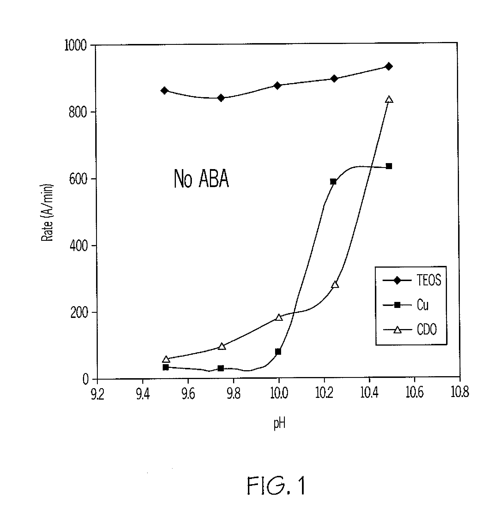
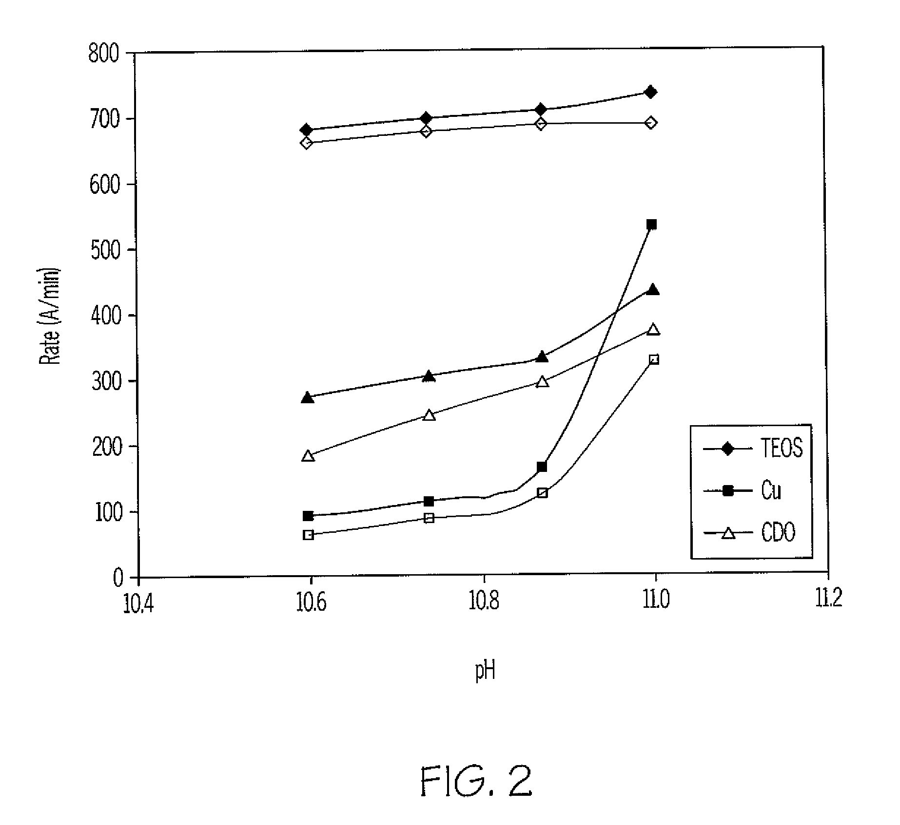
[0035]The above data show that varying BTA, poly(methyl vinyl ether), potassium phosphate and aminobutyric acid concentrations have no dramatic influence in TEOS, CDO and copper removal rates. Referring to FIGS. 1 and 2, FIG. 2 illustrates the removal rate stability achieved with the aminobutyric acid.

example 2

[0036]A second series of slurries varied BTA, poly(methyl vinyl ether), potassium phosphate and aminobutyric acid to determine polishing characteristics. Polishing data are below in Table 3.

TABLE 3CuNon-TEOSCDOCuUniformitySlurry(Å / min)(Å / min)(Å / min)(%)Ta126785574652.3High137166114583.7High147358735083.6High157326774982.3High167518075332.4High1780611245902.3High1882014735793.3HighCDO equals Coral from Novellus; andHigh equals an expected tantalum removal rate of at least 400 Å / Min.

[0037]The above data also show that varying BTA, poly(methyl vinyl ether), potassium phosphate and aminobutyric acid concentrations have no dramatic influence in TEOS, CDO and copper removal rates.

Table 2

example 3

[0038]A third series of slurries varied BTA, poly(methyl vinyl ether), potassium phosphate and aminobutyric acid to determine polishing characteristics for, copper and carbon-doped oxide, including carbon-doped oxide for patterned wafers. Polishing data are below in Table 4.

TABLE 4CuCDONon-PatternedCDOCuUniformityWaferSlurry(Å / min)(Å / min)(%)(Å / min)Ta1920727515320High2011631562354High2117830584366High2218727411378High2315826428305High2420828503407High2514824343266High2617725543354High2720727515320High2811631562354HighCDO equals Coral from Novellus;CDO Patterned Wafer equals Black Diamond from Applied Materials and High equals an expected tantalum removal rate of at least 400 Å / Min.

[0039]The above data show that varying BTA, poly(methyl vinyl ether), potassium phosphate and aminobutyric acid concentrations have no dramatic influence in CDO and copper removal rates. In addition, the above data show that varying BTA, poly(methyl vinyl ether), potassium phosphate and aminobutyric acid co...


PUM

PropertyMeasurementUnit
weight percentaaaaaaaaaa

Abstract

The invention provides a aqueous slurry useful for chemical mechanical polishing a semiconductor substrate having copper interconnects. The slurry comprises by weight percent, 0 to 25 oxidizing agent, 0.1 to 50 abrasive particles, 0.001 to 10 inhibitor for decreasing static etch of the copper interconnects, 0.001 to 5 poly(methyl vinyl ether) having a formula as follows:and the poly(methyl vinyl ether) is water soluble and n has a value of at least 5, 0.005 to 1 aminobutyric acid, 0.01 to 5 phosphorus-containing compound, 0 to 10 copper complexing agent formed during polishing and balance water.

Description

BACKGROUND OF THE INVENTION[0001]As ultra-large-scale-integrated circuit (ULSI) technology migrates to smaller lines widths, there are new challenges for the integration of conventional chemical mechanical polishing (CMP) processes. In addition, the introduction of low k and ultra-low k dielectric films requires the use of a gentler CMP processes due to the films' low mechanical strength and weak adhesion to adjacent layers. Furthermore, ever-tightening defectivity specifications have placed additional demands on polishing slurries for low k films.[0002]The integration of various low k films into USLIs can also require numerous extra steps and the incorporation of new technologies such as supercritical cleaning, dielectric and metal caps, conformal deposition of barriers and copper, chemical mechanical planarization with low down force and abrasive-free slurries. In addition to these technical options, ULSI fabricators must consider and address process complexity versus yield, relia...

Claims


Application Information

Patent Timeline
Patent Type & Authority Applications(United States)
IPC IPC(8): H01L21/465H01L21/463C09K13/00
CPCC09G1/02H01L21/7684H01L21/3212C09K3/1463C09K3/14H01L21/304
Inventor BIAN, JINRU
Owner ROHM & HAAS ELECTRONICS MATERIALS CMP HLDG INC
Learn More