Group iii nitride semiconductor light-emitting device and method of manufacturing the same, and lamp

a technology of nitride and semiconductor light, which is applied in the manufacture of semiconductor/solid-state devices, semiconductor devices, electrical devices, etc., can solve the problems of low light emission efficiency, difficult to obtain, and reduce luminance, so as to enhance light emission efficiency, enhance light extraction efficiency, and enhance light transmittance

Active Publication Date: 2012-01-05
TOYODA GOSEI CO LTD
View PDF0 Cites 15 Cited by
  • Summary
  • Abstract
  • Description
  • Claims
  • Application Information

AI Technical Summary

Benefits of technology

[0017]Accordingly, an object of the present invention is to provide a group III nitride semiconductor light-emitting device which suppresses electric current concentration in a light-transmitting electrode and a semiconductor layer directly below an n-side bonding pad electrode to enhance light emission efficiency, suppresses light absorption in the electrode or light loss due to multiple reflection therein to enhance light extraction efficiency, and has superior external quantum efficiency and electric characteristics.
[0018]It is another object of the present invention to provide a method of manufacturing a group III nitride semiconductor light-emitting device which is capable of manufacturing such a light-emitting device having superior external quantum efficiency and light emission efficiency.
[0019]It is still another object of the present invention to provide a lamp using the above-described group III nitride semiconductor light-emitting device which has superior light emission characteristics.

Problems solved by technology

Thus, as mentioned above, the light emission effect through the light-emitting layer is concentrated directly below the bonding pad electrode, to thereby lower light emission efficiency, which results in reduction in luminance.
However, in the light-emitting devices disclosed in Patent Documents 1 and 2, light emission is relatively strong in the proximity of an n-side bonding pad electrode, and there may be a problem in that it is difficult to obtain a superior electric characteristic, and the light emission efficiency cannot necessarily be enhanced.[Patent Document 1] Japanese Patent No. 3841460[Patent Document 2] JP-A-2008-192710

Method used


Image

  • Group iii nitride semiconductor light-emitting device and method of manufacturing the same, and lamp
  • Group iii nitride semiconductor light-emitting device and method of manufacturing the same, and lamp
  • Group iii nitride semiconductor light-emitting device and method of manufacturing the same, and lamp

Examples


examples

[0184]Next, the group III nitride semiconductor light-emitting device, its method of manufacturing and the lamp according to the present embodiments will be described in more detail below using examples and comparative examples, but the present embodiments are not limitative. [Example 1]

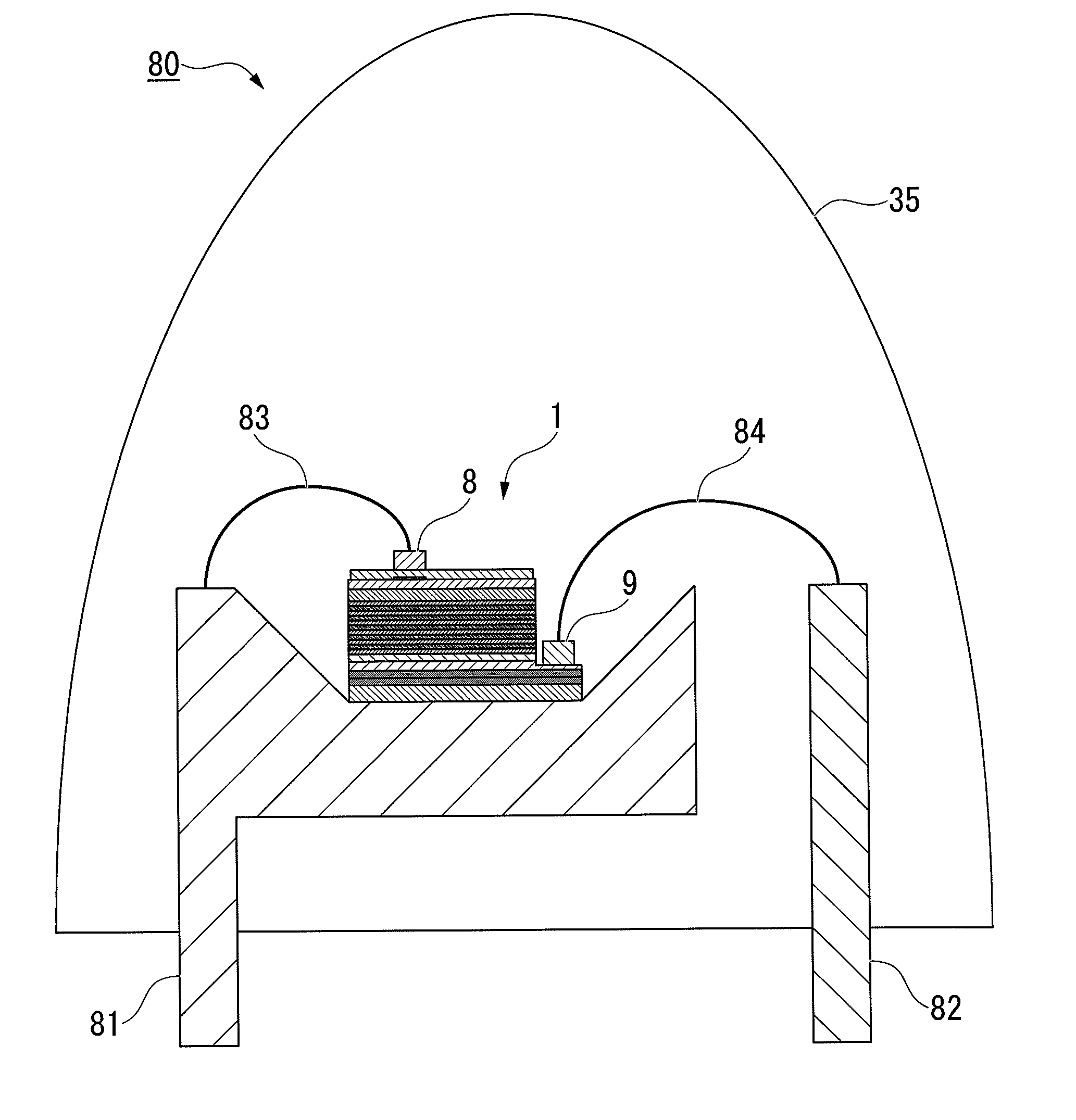
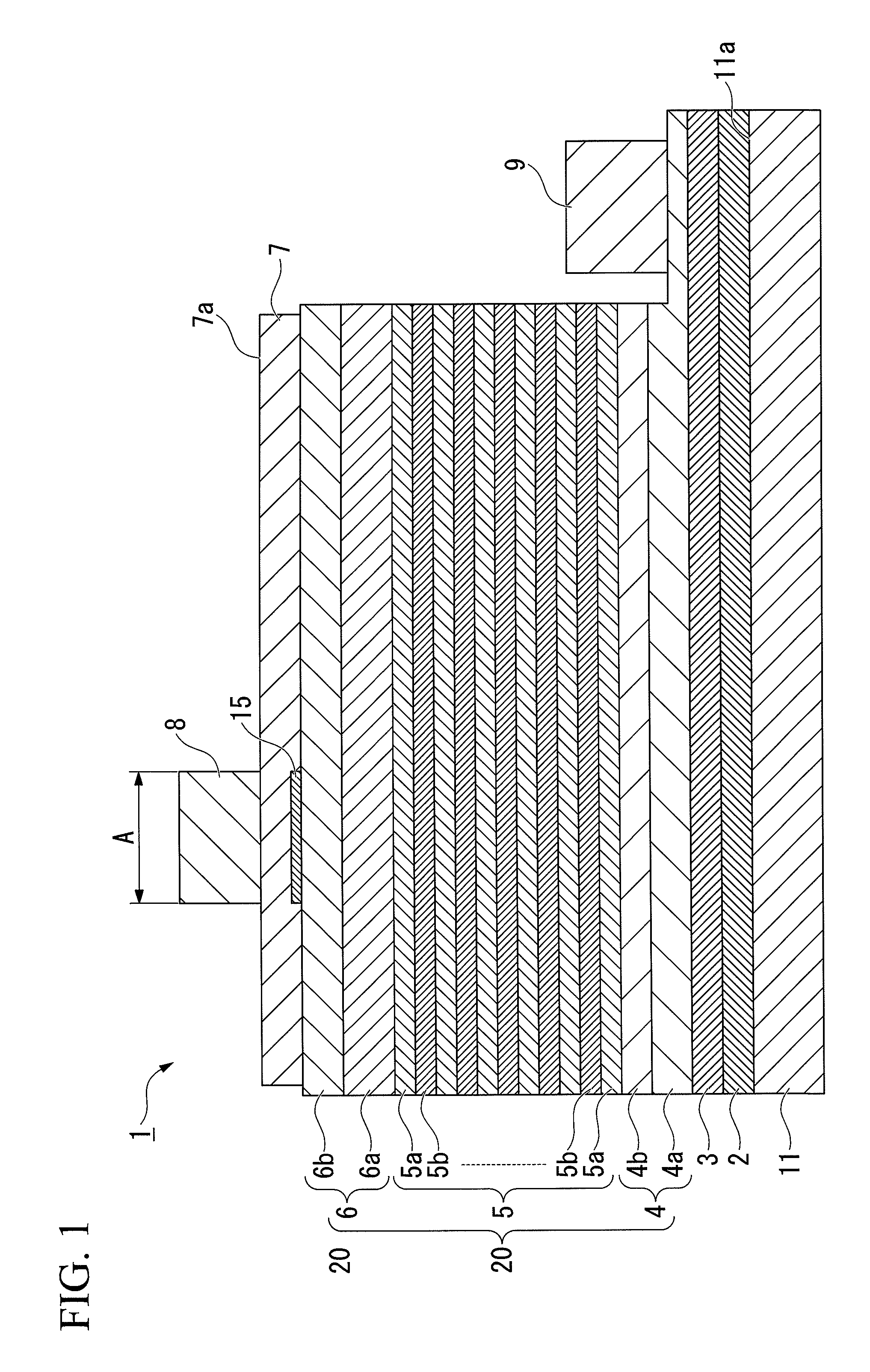
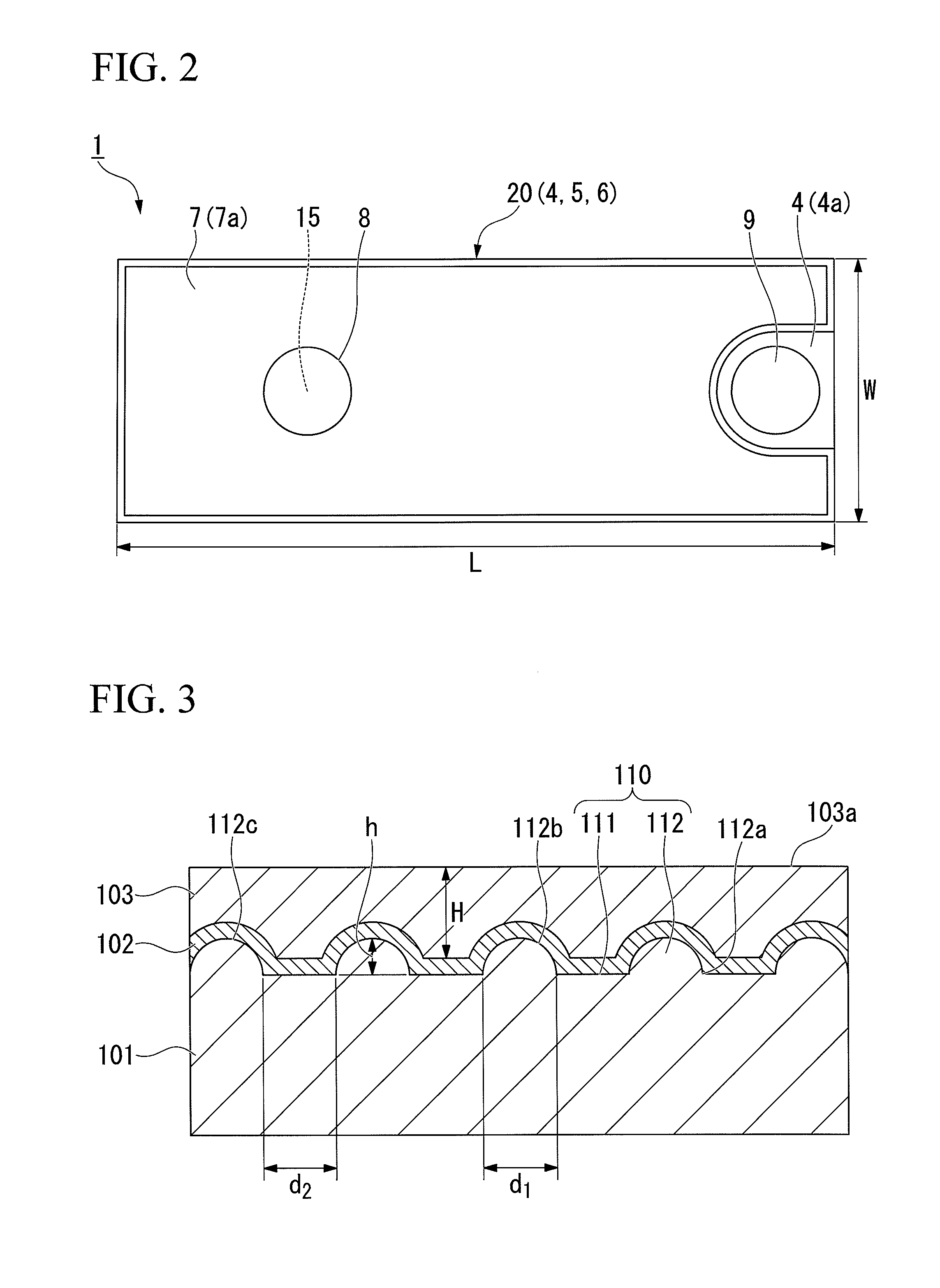
[0185]In this example, samples of the light-emitting device were manufactured in the above-described processes (see FIGS. 1 to 4, FIG. 7 or the like).

[0186]Firstly, the substrate 11 having the main surface 11a formed from the (0001) C plane of a sapphire substrate was prepared. Here, in this example, a substrate in which a plurality of convex portions (not shown) was formed on the main surface 11a was used as the substrate 11 (see the convex portions 112 formed on the main surface 110 in FIGS. 3 and 4). Further, in this example, a substrate was used in which the base width d1 of the convex portion formed on the main surface 11a was 1.3 μm, the height h was 0.7 μm, and the interval d2 was 0.7 μm.

[0187...

examples 2 and 3

, Comparative Examples 1 and 2

[0206]In Examples 2 and 3 and Comparative Examples 1 and 2, under the conditions of the presence or absence of the insulation layer, the film thickness of the light-transmitting electrode, and the distance between centers of the positive electrode bonding pad and the negative electrode bonding pad from a planar view of the wafer, shown in the following Table 1, the chip of the group III nitride semiconductor light-emitting device having a rectangular shape of 240 μm×600 μm was manufactured in a similar way to Example 1, except that the relationship of the respective sheet resistances were appropriately adjusted to be the relationship shown in the following Table 1. Further, similarly, the lamp was manufactured using this chip.

[0207]Further, the light emission output Po (mW) and the drive voltage (Vf) when a forward current of 20 mA flowed between the p-side electrode (positive electrode bonding pad) and the n-side electrode (negative electrode bonding p...

examples 4 to 6

[0209]In Examples 4 to 6, under the conditions of the film thickness of the light-transmitting electrode and the relationship of the respective sheet resistances, shown in the following Table 2, the chip of the group III nitride semiconductor light-emitting device was manufactured in a similar way to Example 1, except that the relationship of the electrode separation direction size (L: chip length) and the chip width (W) in a direction perpendicular to the chip length, from a planar view of the wafer, were appropriately adjusted to be the relationship shown in the following Table 2. Further, similarly, the lamp was manufactured using this chip.

[0210]Further, the light emission output Po (mV) when a forward electric current IF of 30 mA, and as necessary, 100 mA flowed between the p-side electrode (positive electrode bonding pad) and the n-side electrode (negative electrode bonding pad) of the lamp was measured by the same method.

[0211]Specifications of the light-emitting device in Ex...


PUM


Abstract

Disclosed is a group III nitride semiconductor light-emitting device which suppresses electric current concentration in a light-transmitting electrode and a semiconductor layer directly below an electrode to enhance light emission efficiency, suppresses light absorption in the electrode or light loss due to multiple reflection therein to enhance light extraction efficiency, and has superior external quantum efficiency and electric characteristics. A semiconductor layer (20), in which an n-type semiconductor layer (4), a light-emitting layer (5) and a p-type semiconductor layer (6) are sequentially layered, is formed on a single-crystal underlayer (3) which is formed on a substrate (11). A light-transmitting electrode (7) is formed on the p-type semiconductor layer (6). An insulation layer (15) is formed on at least a part of the p-type semiconductor layer (6), and the light-transmitting electrode (7) is formed to cover the insulation layer (15). A positive electrode bonding pad (8) is provided in a position A corresponding to the insulation layer (15) provided on the p-type semiconductor layer (6), on a surface (7a) of the light-transmitting electrode (7). A sheet resistance of the n-type semiconductor layer (4) is lower than a sheet resistance of the light-transmitting electrode (7).

Description

BACKGROUND OF THE INVENTION[0001]1. Technical Field[0002]The present invention relates to a group III nitride semiconductor light-emitting device that has a light-emitting diode (LED) structure and a method of manufacturing the same, and a lamp.[0003]Priority is claimed on Japanese Patent Application No. 2009-054204 filed on Mar. 6, 2009 and Japanese Patent Application No. 2010-46812 filed on Mar. 3, 2010, the content of which is incorporated herein by reference.[0004]2. Background Art[0005]In recent years, a group III nitride semiconductor has been attracting attention as a semiconductor material used for a light-emitting device which emits light of a short wavelength. The group III nitride semiconductor is represented by a general formula AlxGayInzN (0≦x≦1, 0≦y≦1, 0≦z≦1 and x+y+z=1), and is formed on a substrate made of sapphire single-crystal, various kinds of oxides or a group III-V compound, through a metal organic chemical vapor deposition (MOCVD) method, a molecular beam epit...

Claims


Application Information

Patent Timeline
Patent Type & Authority Applications(United States)
IPC IPC(8): H01L33/22
CPCH01L33/007H01L33/42H01L33/145H01L33/025H01L33/32H01L33/36H01L33/38
Inventor HIRAIWA, DAISUKESHINOHARA, HIRONAO
Owner TOYODA GOSEI CO LTD
Why Eureka
Try Eureka