Solid-state imaging device and semiconductor display device

a technology of solid-state imaging and semiconductors, which is applied in the direction of radio frequency controlled devices, instruments, television systems, etc., can solve the problems of signal delay, reduced image quality, and high probability of potential decrease or signal delay along the wiring as stated above, so as to reduce the power consumption of a solid-state imaging device, prevent the variation of the potential of signals, and suppress the potential of decrease or signal delay

Active Publication Date: 2012-01-05
SEMICON ENERGY LAB CO LTD
View PDF8 Cites 58 Cited by
  • Summary
  • Abstract
  • Description
  • Claims
  • Application Information

AI Technical Summary

Benefits of technology

[0023]In one embodiment of the present invention, among wirings for supplying a potential to pixels provided in rows or columns, at least two of a plurality of wirings for supplying a potential to a photodiode, or at least two of a plurality of wirings for supplying a potential of a signal for controlling the switching of the transistor with significantly small off-state current are electrically connected to each other. The above structure can suppress a potential decrease or a signal delay due to wiring resistance and can prevent the above potential or the potential of the signal from varying within a pixel portion. As a result, it is possible to prevent variation in the potential of signals to be output from photosensors, and it is possible to take a high-quality image.
[0024]In one embodiment of the present invention, a global shutter method is employed, so that the above structure can be combined with FS operation. The adoption of FS operation can reduce power consumption of a solid-state imaging device or a semiconductor display device.
[0025]In one embodiment of the present invention, a transistor with significantly small off-state current is used as a switching element for holding charge that is accumulated in a photosensor; accordingly, it is possible to suppress a grayscale change due to a difference in charge holding period and to take a high-quality image, even when the image is taken by a global shutter method.

Problems solved by technology

In addition, a wiring having higher resistance or a contact portion or the like having higher parasitic capacitance is more likely to cause a signal delay.
When a potential decrease or a signal delay along the wiring occurs, the power supply potential or the signal potential to be supplied to photosensors varies within the pixel portion, and the potential variation is reflected in the potential of a signal to be output from the photosensors and reduces the quality of an image to be taken.
However, since all pixels perform accumulation operation simultaneously in the case of the global shutter method, potential decrease or signal delay along a wiring as stated above is highly likely to occur, depending on the current or voltage supply capability of a driver circuit.
In particular, in a portable electronic device such as a mobile phone, a solid-state imaging device or a semiconductor display device is required to consume less power because high power consumption thereof leads to a disadvantage of short continuous operation time.

Method used


Image

  • Solid-state imaging device and semiconductor display device
  • Solid-state imaging device and semiconductor display device
  • Solid-state imaging device and semiconductor display device

Examples


embodiment 1

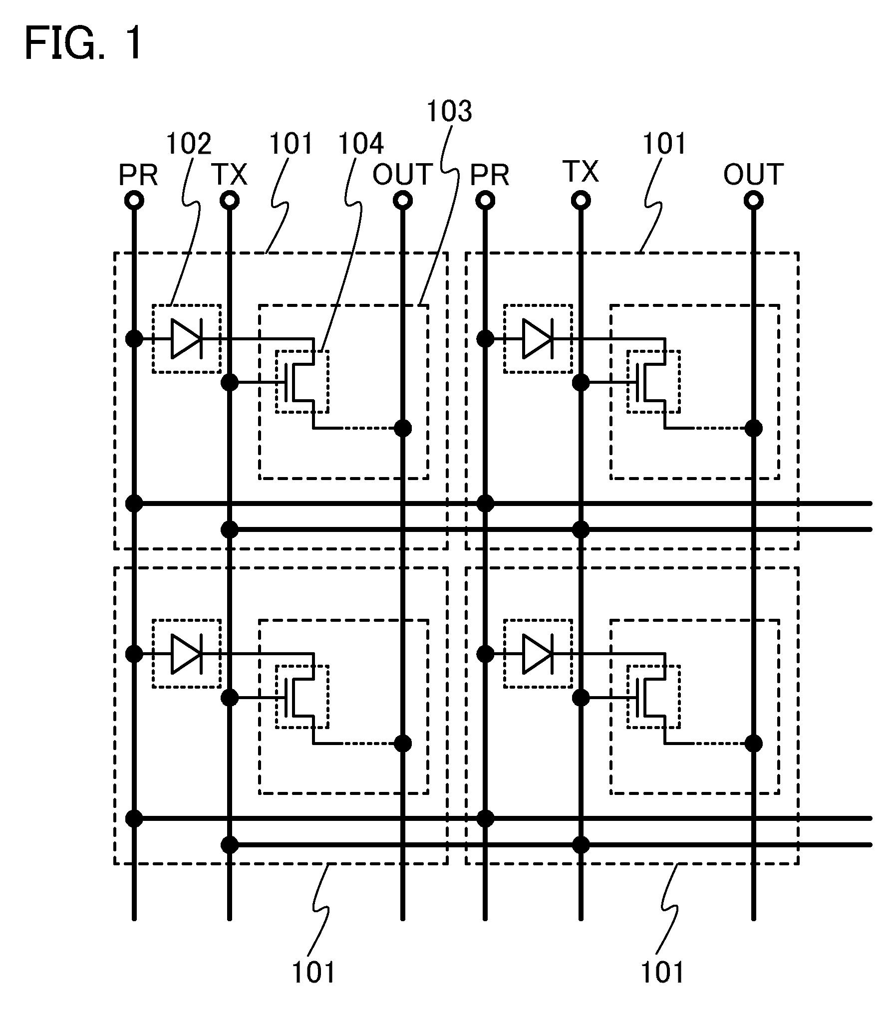
[0047]A configuration of connections among photosensors included in a solid-state imaging device or a semiconductor display device of one embodiment of the present invention will be described with reference to FIG. 1.

[0048]FIG. 1 is an example of a circuit diagram illustrating a configuration of connections among a plurality of photosensors 101 in a pixel portion. In FIG. 1, the photosensors 101 included in pixels are arranged in matrix. Each of the photosensors 101 includes a photodiode 102 and an amplifier circuit 103. The photodiode 102 is a photoelectric conversion element which generates current when a junction of semiconductors is irradiated with light. The amplifier circuit 103 is a circuit which amplifies current obtained through light reception by the photodiode 102 or which holds charge accumulated due to the current.

[0049]The amplifier circuit 103 may have any configuration as long as it can amplify current generated in the photodiode 102; the amplifier circuit 103 includ...

embodiment 2

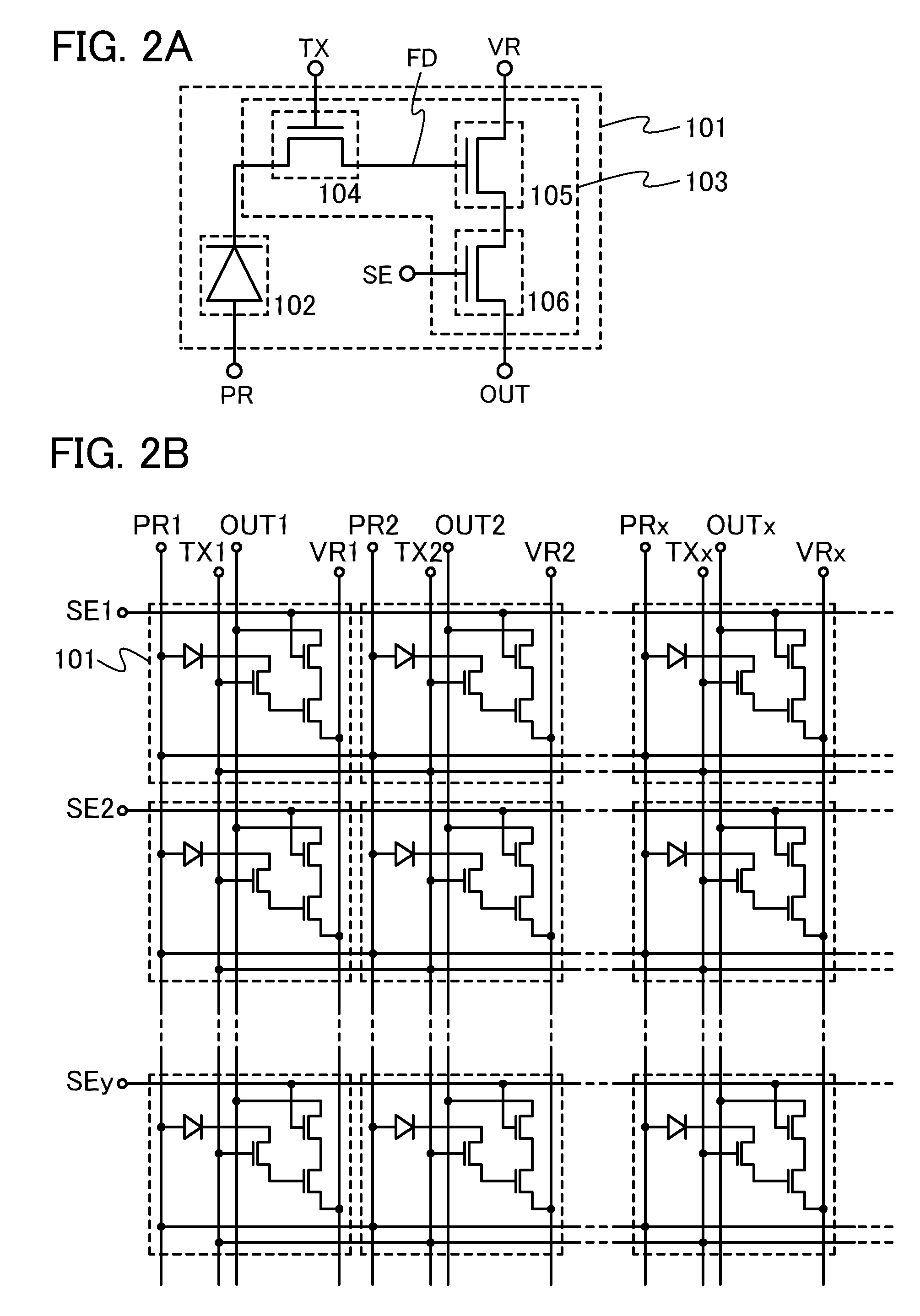
[0155]In this embodiment, a configuration of the photosensor 101 which is different from that in FIG. 2A will be described.

[0156]FIG. 11 is a circuit diagram of an example of the photosensor 101. In the photosensor 101 illustrated in FIG. 11, the amplifier circuit 103 includes a transistor 104, a transistor 105, a transistor 106, and a transistor 107. The transistor 104 controls the supply of current generated in the photodiode 102 to the amplifier circuit 103. In the transistor 105, the current value or resistance value between a first terminal and a second terminal thereof is determined by a potential supplied to the second terminal of the transistor 104. The transistor 106 functions as a switching element for supplying a potential of an output signal determined by the current value or resistance value, to the wiring OUT. The transistor 107 functions to reset the amount of charge accumulated in the amplifier circuit 103.

[0157]Specifically, in FIG. 11, a first terminal of the trans...

embodiment 3

[0176]In this embodiment, a method for manufacturing a solid-state imaging device or a semiconductor display device according to one embodiment of the present invention, which has a transistor including silicon and a transistor including an oxide semiconductor, will be described.

[0177]Note that in one embodiment of the present invention, an oxide semiconductor may be used for a transistor included in an amplifier circuit, or a general semiconductor such as germanium, silicon, silicon germanium, or single crystal silicon carbide may be used. For example, the transistor including silicon can be formed using a single crystal semiconductor substrate such as a silicon wafer or the like, a silicon thin film which is formed by an SOI method, a silicon thin film which is formed by a vapor deposition method, or the like.

[0178]First, as illustrated in FIG. 14A, a photodiode 704 and an n-channel transistor 705 are formed over an insulating surface of a substrate 700 by a known CMOS fabricating...


PUM


Abstract

An object is to provide a solid-state imaging device or a semiconductor display device with which a high-quality image can be taken. By performing operation using a global shutter method, a potential for controlling charge accumulation operation can be shared by all pixels. In addition, a first photosensor group includes a plurality of photosensors connected to a wiring supplied with an output signal, and a second photosensor group includes a plurality of photosensors connected to another wiring supplied with the output signal. A wiring for supplying a potential or a signal for controlling charge accumulation operation to the first photosensor group is connected to a wiring for supplying the potential or signal to the second photosensor group.

Description

BACKGROUND OF THE INVENTION[0001]1. Field of the Invention[0002]An embodiment of the present invention relates to a solid-state imaging device including a photosensor in a pixel, and to a semiconductor display device including a photosensor and a display element in a pixel.[0003]2. Description of the Related Art[0004]A photosensor utilizing an amplifying function of a MOS transistor, called a CMOS sensor, can be manufactured by a general CMOS process. Thus, manufacturing cost of a solid-state imaging device including a CMOS sensor in each pixel can be low, and a semiconductor display device having a photosensor and a display element formed over one substrate can be realized. In addition, a CMOS sensor requires lower driving voltage than a CCD sensor; therefore, power consumption of the solid-state imaging device can be suppressed.[0005]For a solid-state imaging device or a semiconductor display device including a CMOS sensor, a rolling shutter method is generally employed in which a...

Claims


Application Information

Patent Timeline
Patent Type & Authority Applications(United States)
IPC IPC(8): H04N5/335G09G5/00
CPCG09G3/3413G09G3/3648G09G2300/0876G09G2310/0235H04N5/3745H01L27/1225H04N5/353H04N5/3696H04N5/3741G09G2320/0261H04N25/53H04N25/702H04N25/766H04N25/77H01L27/146H04N25/62H04N25/76
Inventor AOKI, TAKESHITAMURA, HIKARUIKEDA, TAKAYUKIKUROKAWA, YOSHIYUKI
Owner SEMICON ENERGY LAB CO LTD
Why Eureka
Try Eureka