Intrinsic Programming Current Control for a RRAM

a current control and programming technology, applied in the field of switching devices, can solve the problems of increasing power dissipation, preventing proper device operation, and non-scaling of sub-threshold slopes, and achieve the effect of high enduran

Inactive Publication Date: 2012-01-12
CROSSBAR INC
View PDF3 Cites 108 Cited by
  • Summary
  • Abstract
  • Description
  • Claims
  • Application Information

AI Technical Summary

Benefits of technology

[0008]The present invention is related to switching devices. More particularly, the present invention provides a structure and a method for forming a r

Problems solved by technology

However, as field effect transistors (FET) approach sizes less than 100 nm, problems such as short channel effect start to prevent proper device operation.
Moreover, such sub 100 nm device size can lead to sub-threshold slope non-scaling and also increases power dissipation.
These devices often require new materials and device structures to couple with silicon based devices to form a memory cell, which lack one

Method used


Image

  • Intrinsic Programming Current Control for a RRAM
  • Intrinsic Programming Current Control for a RRAM
  • Intrinsic Programming Current Control for a RRAM

Examples


Embodiment Construction

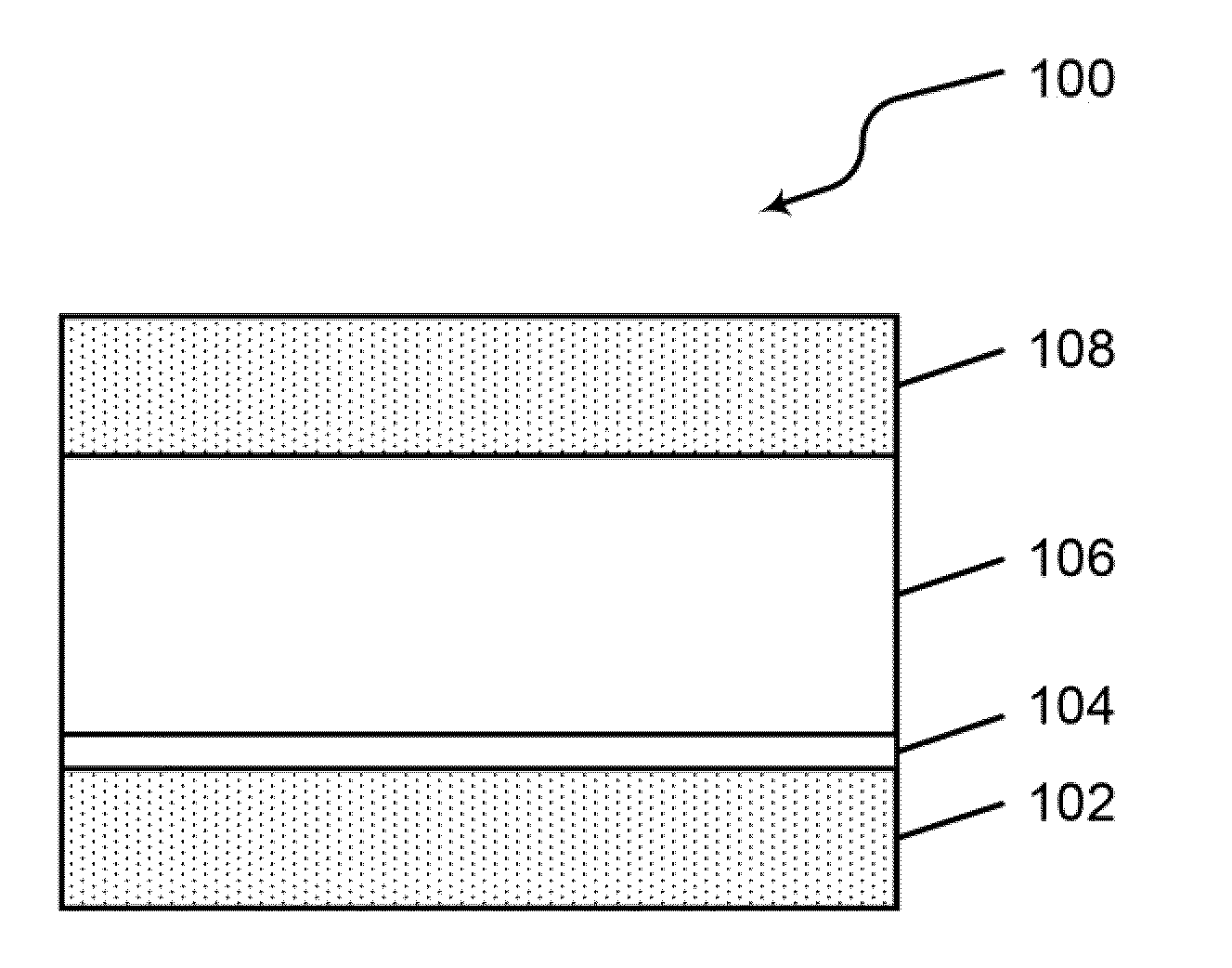
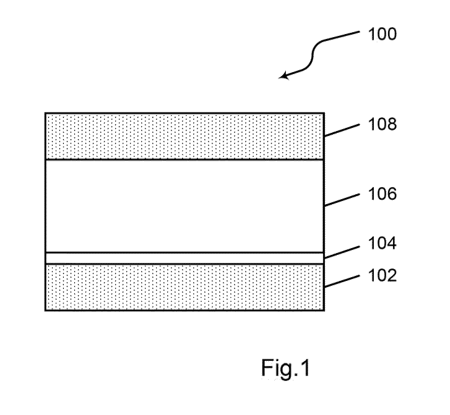
[0016]The present invention is related to switching devices. More particularly, the present invention provides a structure and a method for forming a resistive switching memory device. The resistive switching memory device is characterized by an intrinsic programming current control and high endurance.

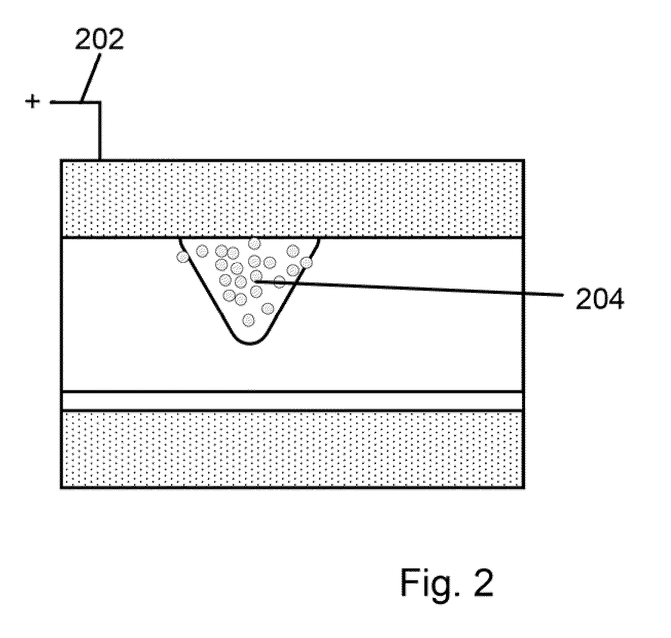
[0017]Resistive switching in an amorphous silicon based resistive random access memory (RRAM) is caused by metal particle injection from a metal electrode into the amorphous silicon material. When the device is in on state, the metal particles form a filament structure in the amorphous silicon material. When a voltage is applied, electrons can tunnel from one metal particle to a neighboring metal particle allowing a tunneling current to flow along the filament structure. At an off state, the filament structure becomes discontinued that very low current flows in the amorphous silicon material and the device is in a high resistance state. As tunneling current has an exponential dependenc...


PUM


Abstract

A resistive switching device. The device includes a substrate and a first dielectric material overlying a surface region of the substrate. The device includes a first electrode overlying the first dielectric material and an optional buffer layer overlying the first electrode. The device includes a second electrode structure. The second electrode includes at least a silver material. In a specific embodiment, a switching material overlies the optional buffer layer and disposed between the first electrode and the second electrode. The switching material comprises an amorphous silicon material in a specific embodiment. The amorphous silicon material is characterized by a plurality of defect sites and a defect density. The defect density is configured to intrinsically control programming current for the device.

Description

CROSS REFERENCE TO RELATED APPLICATIONS[0001]N / ASTATEMENT RELATED TO FEDERALLY SPONSORED RESEARCH OR DEVELOPMENT[0002]N / AREFERENCE TO A “SEQUENCE LISTING,” A TABLE, OR A COMPUTER PROGRAM LISTING APPENDIX SUBMITTED ON COMPACT DISC[0003]N / ABACKGROUND[0004]The present invention is related to switching devices. More particularly, the present invention provides a structure and a method for forming a resistive switching memory device. The resistive switching memory device is characterized by an intrinsic programming current control and high endurance, among others.[0005]The success of semiconductor devices has been mainly driven by an intensive transistor down-scaling process. However, as field effect transistors (FET) approach sizes less than 100 nm, problems such as short channel effect start to prevent proper device operation. Moreover, such sub 100 nm device size can lead to sub-threshold slope non-scaling and also increases power dissipation. It is generally believed that transistor ...

Claims


Application Information

Patent Timeline
IPC IPC(8): H01L45/00H01L21/02
CPCH10N70/245H10N70/841H10N70/884H10N70/023
Inventor JO, SUNG HYUNLU, WEI
Owner CROSSBAR INC
Why Eureka
Try Eureka