
Organic electroluminescent device, method for manufacturing organic electroluminescent device, image display device, and method for manufacturing image display device

an image display device and organic technology, applied in the direction of thermoelectric device junction materials, semiconductor devices, electrical apparatus, etc., can solve the problems of unevenness in images shown by image display devices, low throughput, and difficulty in obtaining the desired level of patterning precision, so as to reduce the unevenness of luminescence

Inactive Publication Date: 2012-01-12
TOPPAN PRINTING CO LTD
View PDF4 Cites 51 Cited by
  • Summary
  • Abstract
  • Description
  • Claims
  • Application Information

AI Technical Summary

Benefits of technology

[0055]According to the first and second embodiments of the present invention, a recessed and projected shape is formed on the surface of a partition wall. As a result, even if a luminescent medium layer is formed on the entire surface of the display region, a displaying abnormality due to a leak current does not occur. In this way, it is possible to manufacture an EL device having good EL characteristics as well.
[0067]Incidentally, it is not necessary to provide a discontinuous island-like part (island-like structure) to the entire surface of the hole transport layer. The island-like structure may be provided only at one portion. For example, the island-like structure may be provided only on the partition wall. As another example, the island-like structure may be provided only on the electrode. As a result, it is possible to use a lot of material as the electrode material, partition wall material, and the hole transport material.

Problems solved by technology

However, there is a problem with such a patterning method in that, as the area of the substrate increases, it becomes more difficult to obtain a desired level of precision in the patterning.
In addition, since a film is formed in a vacuum, there is a problem in that a throughput is low.
As a result, an unevenness may appear in an image shown by an image display device including the hole transport layer or the organic luminescent layer.
However, when these wet coating methods are used, it is difficult to perform a patterning with a thin film at a high level of precision.
It is also difficult to form a thin film by applying three colors including R, G, and B individually.
Therefore, a method using a hard block such as a metallic printing block, like the gravure printing method, is not suitable as a method for forming a polymer organic EL element.
However, the brightness or the efficiency declines due to the driving condition being continued or preserved for a long period of time.
The durability of the organic EL element is low because the heat resistant property of the thin film including TPD, which is a low molecular organic compound material, is low.
The durability of the organic EL element is low also because the molecules within the non-crystallized thin film are altered due to the application of electrical current and becomes a microcrystallite, thereby reducing the functionality.
However, it is difficult to satisfy all of the characteristics that are required.
Even if a material satisfying the required characteristics of work function and band gap is used, a problem occurs as described below, if the specific resistance is low.
Furthermore, according to an image display device configured with an organic EL element as described above, there is a problem in that, when a leak current runs between adjacent pixels, it becomes difficult to control the display in a desirable manner.
When the film thickness exceeds 20 nm, it becomes difficult to form a hole transport layer with an island-like structure.
As a result, when an inorganic material having a low specific resistance is used, a leak current is more likely to occur.
When the film thickness exceeds 20 nm, it becomes difficult to form a hole transport layer with an island-like structure.
As a result, when an inorganic material having a low specific resistance is used, a leak current is more likely to occur.

Method used


Image

  • Organic electroluminescent device, method for manufacturing organic electroluminescent device, image display device, and method for manufacturing image display device
  • Organic electroluminescent device, method for manufacturing organic electroluminescent device, image display device, and method for manufacturing image display device
  • Organic electroluminescent device, method for manufacturing organic electroluminescent device, image display device, and method for manufacturing image display device

Examples


first embodiment

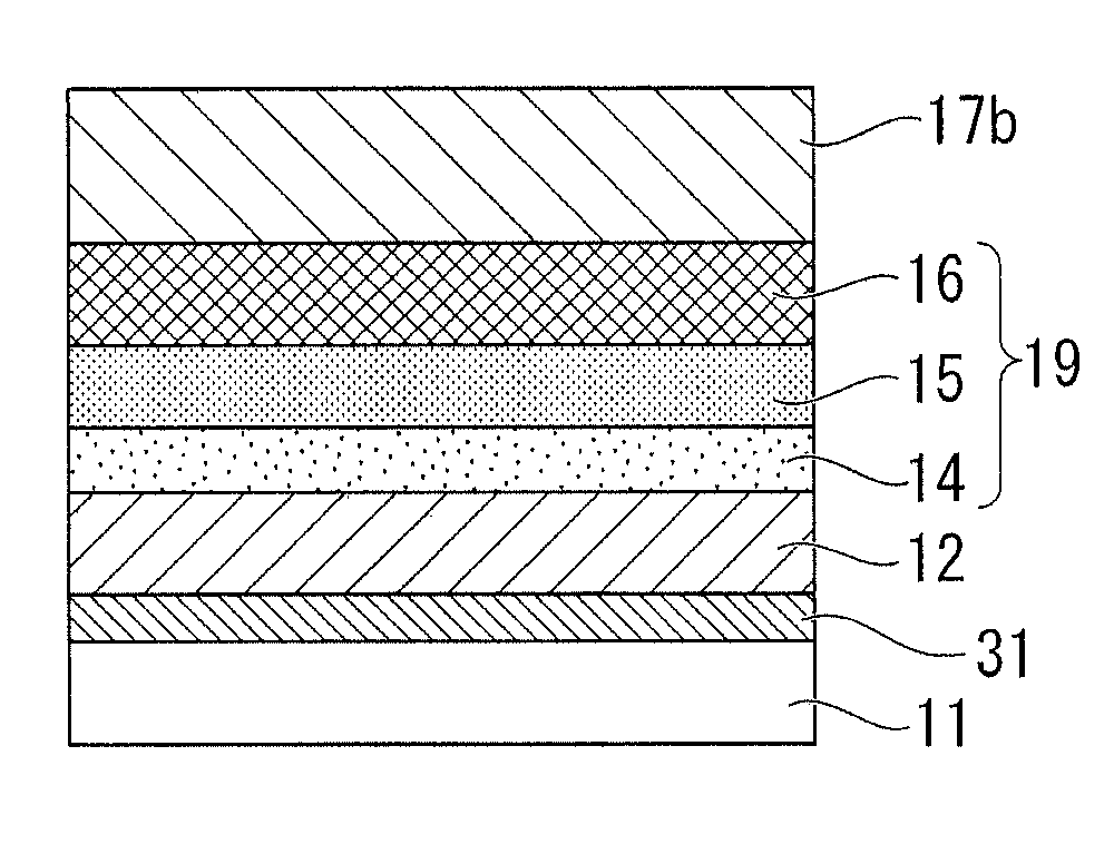
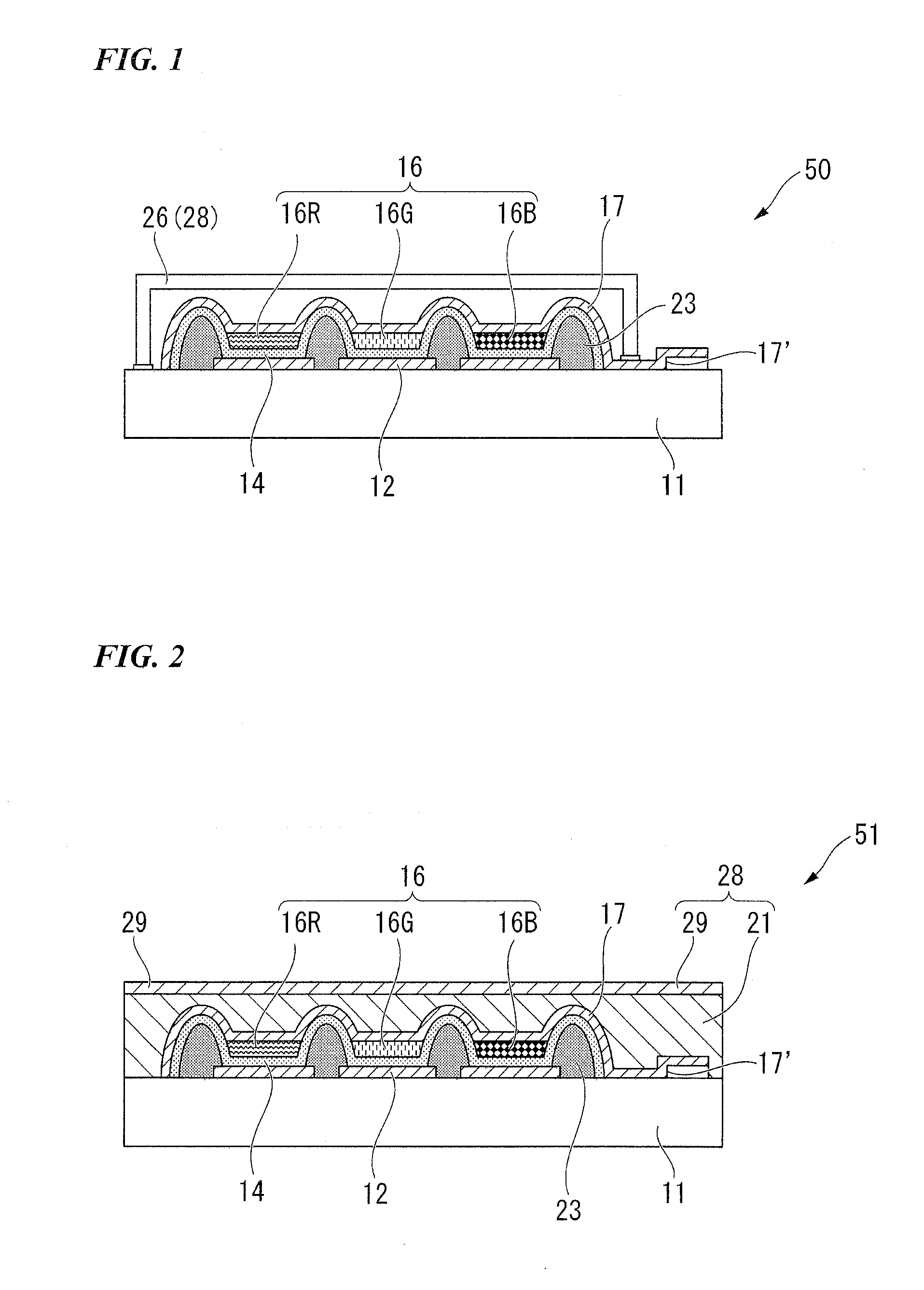
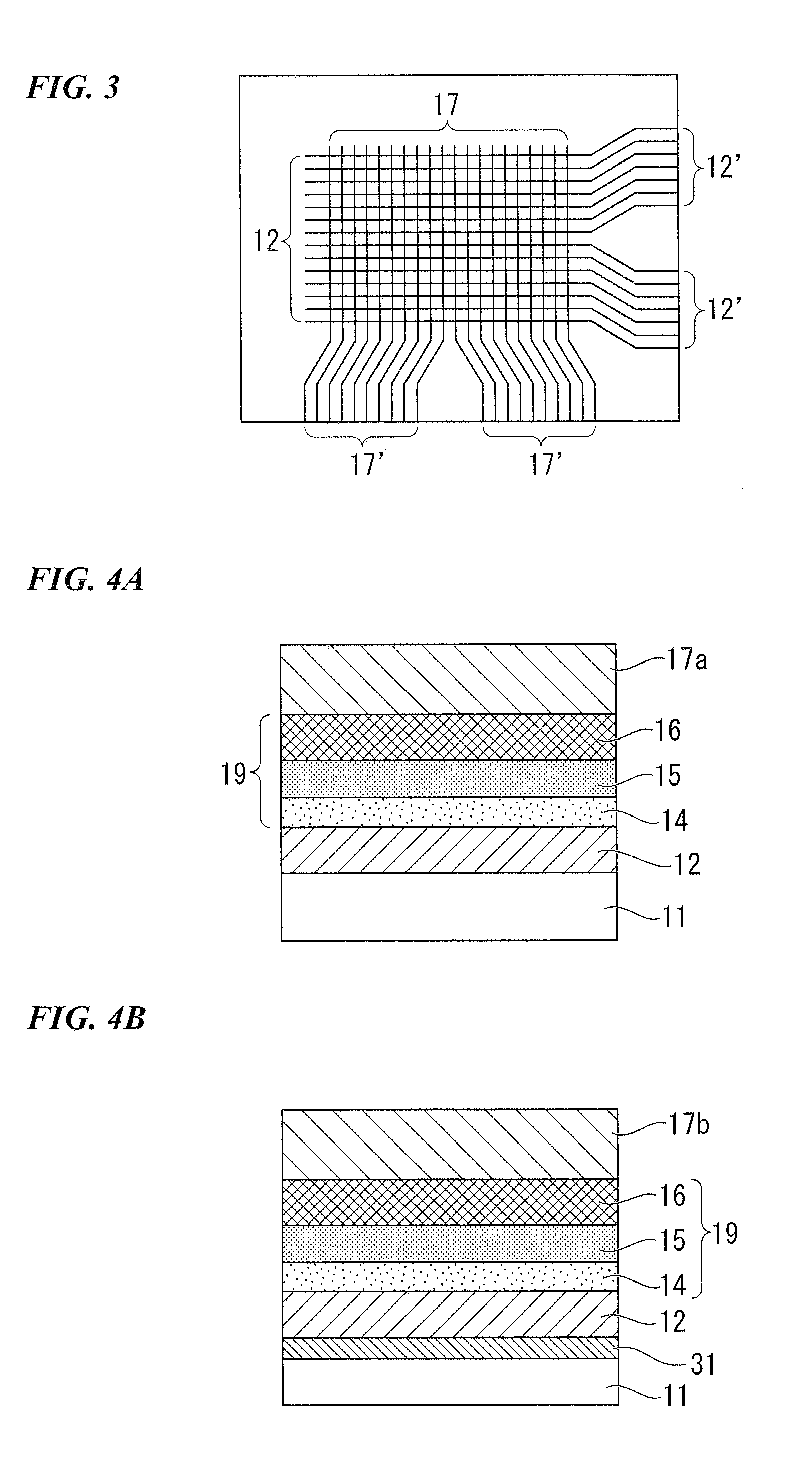
[0099]FIG. 1 is a cross sectional diagram showing a configuration of an organic EL display device (organic electroluminescent device) according to a first embodiment of the present invention.

[0100]FIG. 1 shows a display device 50 using an organic EL element according to a first embodiment of the present invention. The display device 50 includes a substrate 11, a first electrode (positive electrode, pixel electrode) 12, a partition wall 23, a hole transport layer 14, an organic luminescent layer 16, a second electrode (negative electrode) 17, a luminescent medium layer 19 (see FIG. 4A), and a sealing body 28. The first electrode 12 is provided on each pixel on the substrate 11. The partition wall 23 partitions between pixels of the first electrode 12. The hole transport layer 14 is formed above the first electrode 12. The organic luminescent layer 16 is formed on the hole transport layer. The second electrode 17 is formed so as to cover the entire surface of the luminescent layer. Th...

second embodiment

[0189]Next, the second embodiment is described.

[0190]In the description of the second embodiment, the same components described in the first embodiment are referred to using the same reference number. Descriptions of such components may be omitted or simplified. Furthermore, as long as the configuration of the first embodiment is consistent with the configuration of the second embodiment, the configuration described in the first embodiment is also applied to the second embodiment.

[0191]FIG. 8A is a cross sectional view of an organic electroluminescent element (organic EL element) according to the second embodiment of the present invention.

[0192]According to the organic EL element 100 shown in FIG. 8A based on the second embodiment, a luminescent medium layer 109 is provided between the first electrode 102 and the second electrode 107. The luminescent medium layer 109 includes the luminescent layer 106 and the hole transport layer 104. Other than the luminescent layer 106 and the hol...

working example

[0283]Next, a working example of an organic EL display device according to the first and second embodiments described above is described. The present invention is not limited to the following working examples.

[0284]First, referring to working examples 1 through 3 and comparative example 1, a working example of an organic EL display device according to the first embodiment is described.


PUM


Abstract

Provided is an organic electroluminescent device including: a substrate (11, 101); a first electrode (12, 102) formed on the substrate (11, 101) and including a pixel region; a partition wall (23, 203) formed on the substrate (11, 101), partitioning the first electrode (12, 102), and including a surface with a recessed and projected form; a luminescent medium layer (19, 109) formed on the pixel region and the partition wall (23, 203), a film thickness of the partition wall (23, 203) being uneven according to the recessed and projected form; and a second electrode (17, 107) formed on the luminescent medium layer (19, 109).

Description

CROSS REFERENCE TO RELATED APPLICATIONS[0001]This application is a continuation application based on PCT Patent Application No. PCT / JP2010 / 002127, filed Mar. 25, 2010, whose priority is claimed on Japanese Patent Application No. 2009-073551, filed Mar. 25, 2009; Japanese Patent Application No. 2009-073567, filed Mar. 25, 2009; and Japanese Patent Application No. 2009-169849, filed Jul. 21, 2009; the entire contents of which are incorporated herein by reference.BACKGROUND OF THE INVENTION[0002]1. Field of the Invention[0003]The present invention relates to an organic electroluminescent device, a method for manufacturing an organic electroluminescent device, an image display device, and a method for manufacturing an image display device.[0004]2. Description of the Related Art[0005]In recent years, an organic electroluminescent element (hereinafter referred to as an organic EL element) has been developed. The organic EL element is a luminescent element which can emit high-intensity lig...

Claims


Application Information

Patent Timeline
IPC IPC(8): H01L51/52H01L51/56
CPCH01L51/5206H10K59/122H10K50/17H10K50/15H10K71/00H10K59/8051H10K50/81
Inventor KANETA, SHINGOYASU, YUKISYODA, RYOMORIKAWA, NORIKOKITAZUME, EIICHI
Owner TOPPAN PRINTING CO LTD
Features
  • Generate Ideas
  • Intellectual Property
  • Life Sciences
  • Materials
  • Tech Scout
  • Unparalleled Data Quality
  • Higher Quality Content
  • 60% Fewer Hallucinations
Learn More