
Hybrid vertical-cavity laser

a laser and vertical cavity technology, applied in the direction of lasers, laser optical resonators, instruments, etc., can solve the problems of non-intrusive single mode control, high power consumption, and need for tedious alignment and subsequent packaging, so as to reduce unwanted scattering loss, increase overall routing efficiency, and reduce the effect of scattering loss

Inactive Publication Date: 2012-01-12
DANMARKS TEKNISKE UNIV
View PDF7 Cites 56 Cited by
  • Summary
  • Abstract
  • Description
  • Claims
  • Application Information

AI Technical Summary

Benefits of technology

[0012]An example of a prior art VCSEL using two dimensional (2D) grating mirrors can be found in e.g. US 2007 / 0201526. This structure differs from the present invention in several ways, one of them being that one of the end mirrors has a reduced reflectivity in order to function as an output coupler, making the laser surface emitting. Further, US 2007 / 0201526 provides no in-plane waveguide structure in the layer holding the 2D grating structure intended to laterally output light. None the less, the technology is similar and extensive references to VCSEL technology is made throughout the present description. The invention is thereby also advantageous as it applies matured VCSEL technologies exhibiting very low power consumption, eminent single-mode property and mode control in general. Further, the use of VCSEL technology allows for uncomplicated packaging.
[0051]It is further preferred that definition of an optical gain region of the VCL is performed after arranging of the partial VCL structure on the silicon layer. This provides the advantage that the optical gain region can be defined to have the desired overlap with the periodic refractive index grating after the assembly, typically performed by wafer bonding, where they do no more move in relation to each others. This means that little or no aligning effort is necessary during the assembly. The position of the optical gain region of the VCL involves defining a current aperture or similar for directing charge carriers to a delimited part of the active region of the VCL structure.

Problems solved by technology

This approach has the disadvantages that tedious alignment and subsequent packaging is necessary.
While solutions based on edge-emitting lasers provides easier coupling to photonic circuitry, they have the disadvantages of relatively high power consumption and non-intrinsic single mode control.

Method used


Image

  • Hybrid vertical-cavity laser
  • Hybrid vertical-cavity laser
  • Hybrid vertical-cavity laser

Examples


Embodiment Construction

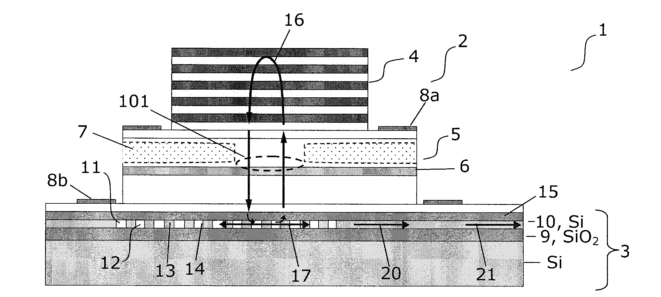
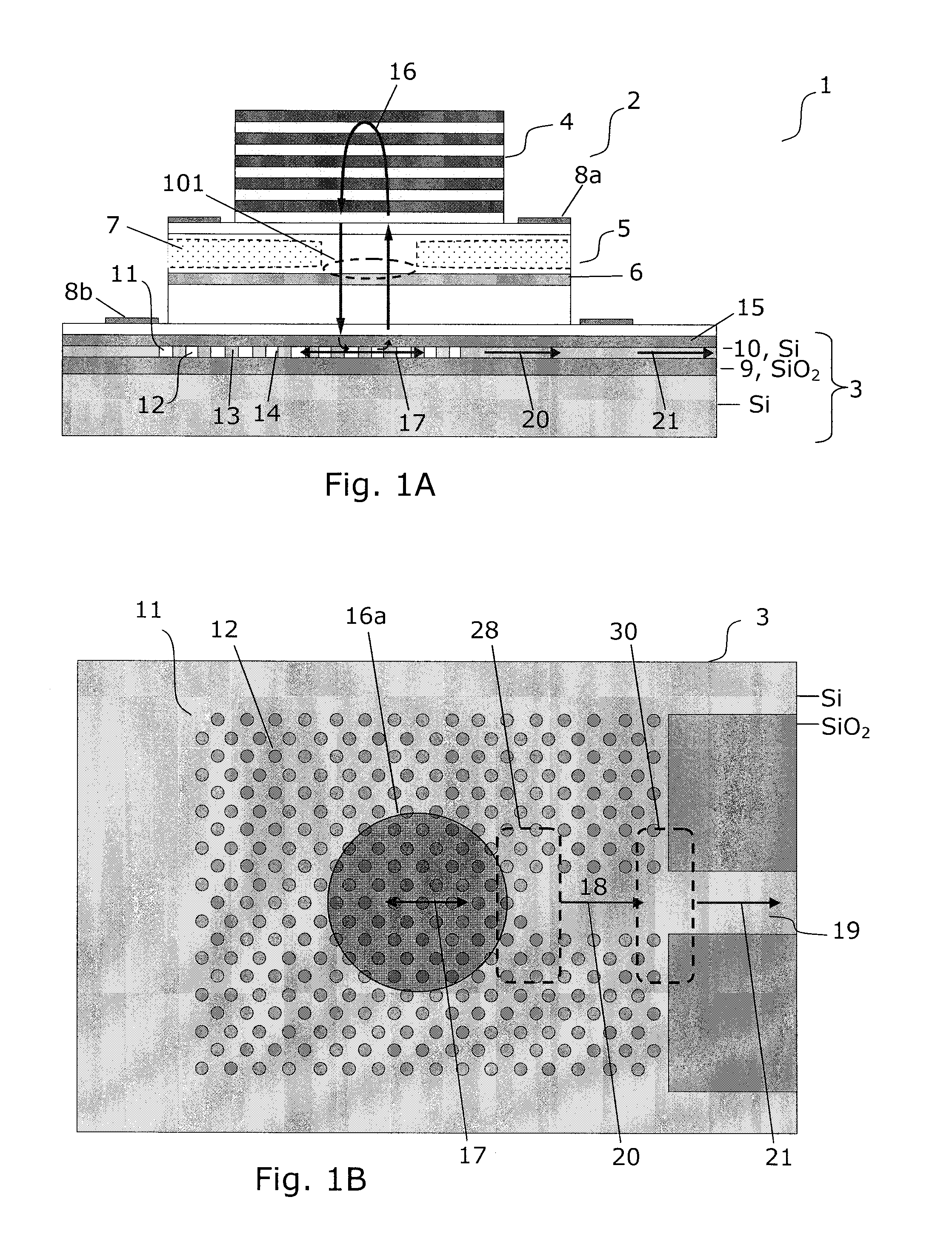
[0062]FIGS. 1A and B illustrate a hybridized grating-mirror vertical-cavity laser (VCL) structure as well as a method for hybridising a grating-mirror vertical-cavity laser (VCL) structure on a silicon platform, according to preferred embodiments of the present invention.

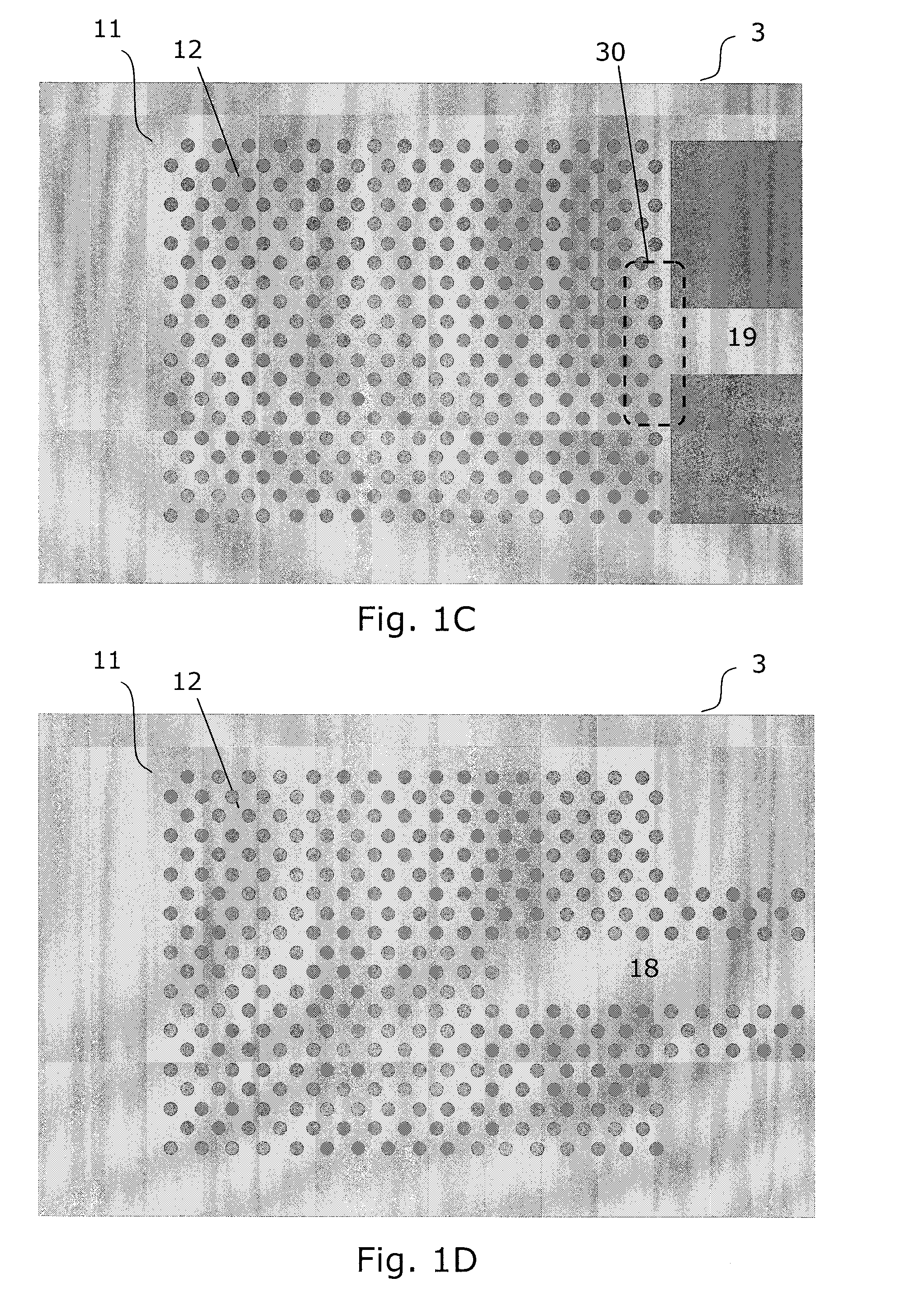
[0063]First, an assembled structure and operating principles are described in relation to FIGS. 1A-C. In FIG. 1A, a hybridised VCL structure 1 is shown, comprising a partial VCL structure 2 and a silicon platform substrate 3.

[0064]The partial VCL structure 2 comprises a highly reflective top mirror 4, here embodied by a distributed Bragg reflector (DBR) being a stack of alternating layers with different refractive indices. DBRs are commonly used top mirrors for VCSEL and their reflectivity can be finely tuned, and can be formed in III-V materials as well as other materials including SiO2.

[0065]For normal VCSELs, the top mirror serves as the out-coupling mirror, and typically has a reflectivity higher than 99% but lo...


PUM


Abstract

The present invention provides a light source (2) for light circuits on a silicon platform (3). A vertical laser cavity is formed by a gain region (101) arranged between a top mirror (4) and a bottom grating-mirror (12) in a grating region (11) in a silicon layer (10) on a substrate. A waveguide (18, 19) for receiving light from the grating region (11) is formed within or to be connected to the grating region, and functions as an 5 output coupler for the VCL. Thereby, vertical lasing modes (16) are coupled to lateral in-plane modes (17, 20) of the in-plane waveguide formed in the silicon layer, and light can be provided to e.g. photonic circuits on a SOI or CMOS substrate in the silicon.

Description

FIELD OF THE INVENTION[0001]The present invention relates to providing light to photonic circuits on a silicon platform that is compatible with matured silicon processing technologies. In particular, the invention relates to providing light to such circuitry by use of a grating-mirror vertical-cavity laser.BACKGROUND OF THE INVENTION[0002]The challenge of integrating small and efficient electrically pumped light sources in silicon based photonic circuitry is well known.[0003]Gunn (Photonics Spectra March 2006, pp. 62-67) described this challenge and proposes a solution where light is provided from non-integrated external laser sources. Through an optical fibre, the light is directed to an integrated holographic lens and thereby coupled to an integrated waveguide. This approach has the disadvantages that tedious alignment and subsequent packaging is necessary.[0004]Fang et al. (Optics Express 14, pp. 9203 (2006)) describes an edge-emitting electrically pumped AlGaInAs-silicon evanesc...

Claims


Application Information

Patent Timeline
IPC IPC(8): H01S5/323H01S5/183G02B5/18H01L33/60
CPCH01S5/021H01S5/0215H01S5/026H01S5/10H01S5/1032H01S5/1838H01S5/18311H01S5/18341H01S5/18366H01S5/3095H01S5/105H01S5/11H01S5/18361H01S5/18386
Inventor CHUNG, IL-SUG
Owner DANMARKS TEKNISKE UNIV
Learn More