

Gate driving circuit for power semiconductor element
a driving circuit and semiconductor technology, applied in the direction of pulse generators, emergency protective arrangements for limiting excess voltage/current, pulse techniques, etc., can solve the problems of hard interruption of igbt b>1/b>, rapid decrease of voltage vg, and noise generation of igbt b>1/b>, so as to avoid device breakdown and suppress noise generation
- Summary
- Abstract
- Description
- Claims
- Application Information
AI Technical Summary
Benefits of technology
Problems solved by technology
Method used
Image

Examples
example 1
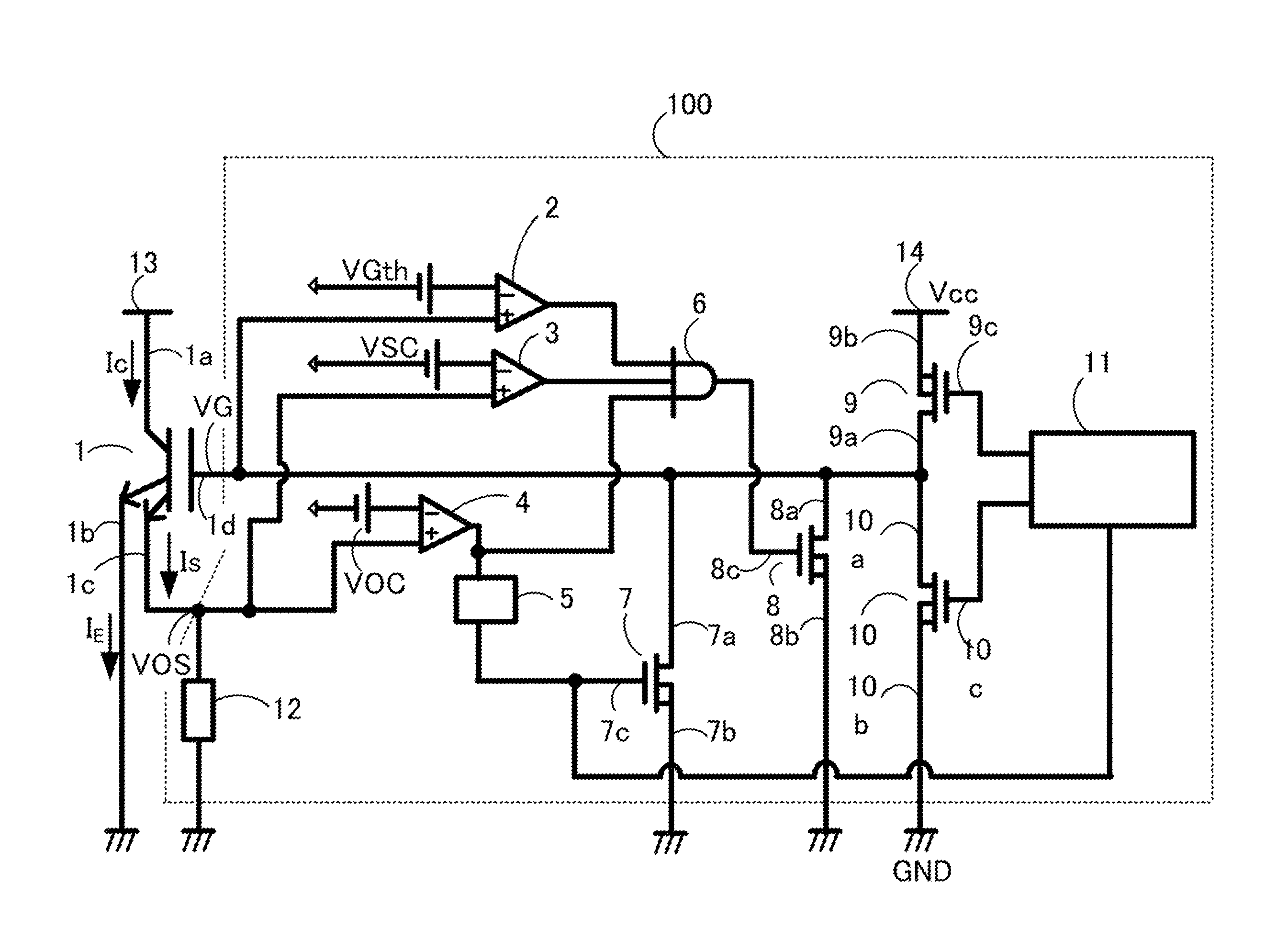
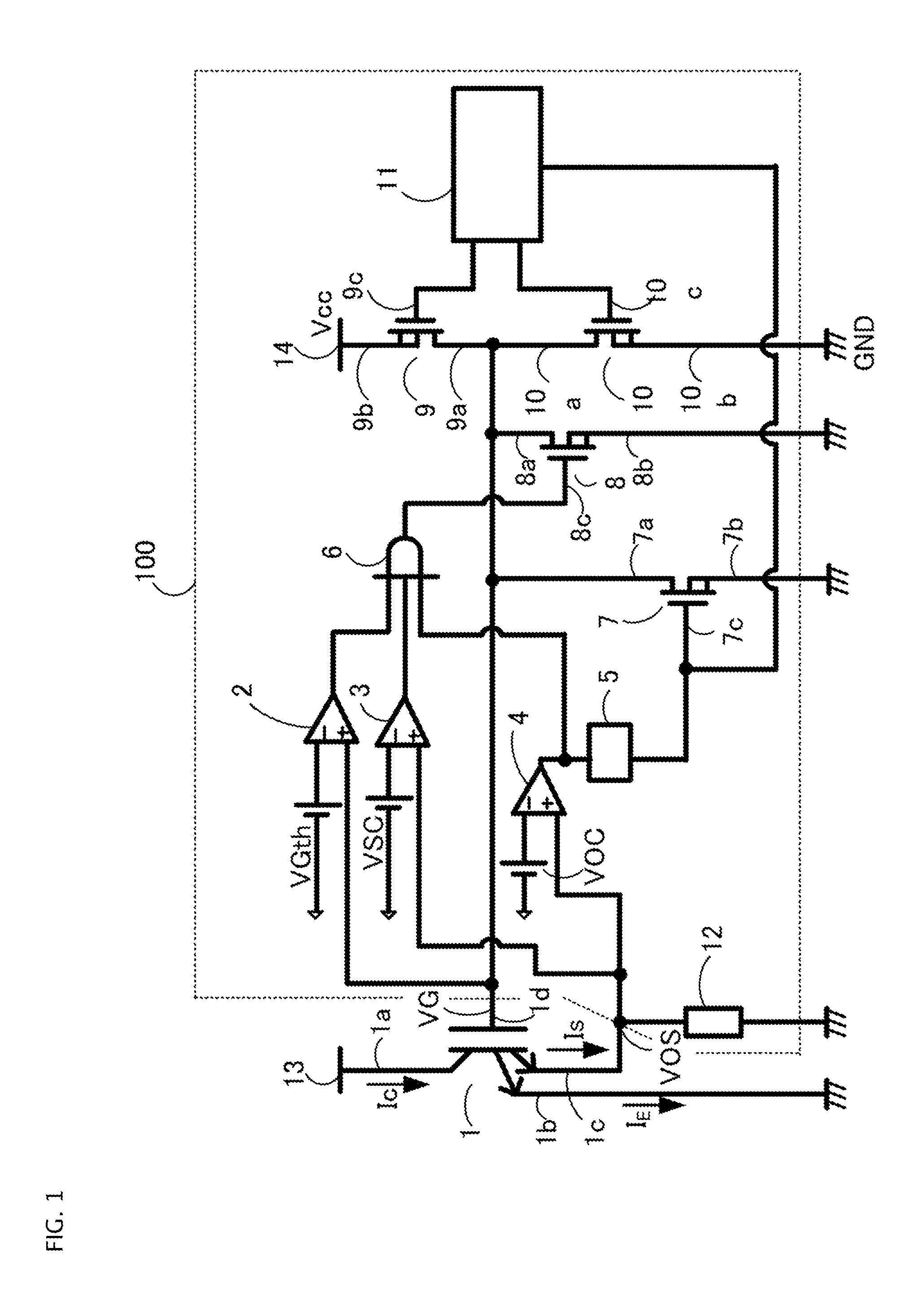
[0048]FIG. 1 is a circuit diagram of an essential part of a gate driving circuit for a power semiconductor element of a first embodiment according to the invention. A power semiconductor element is an IGBT 1 in this embodiment example. The IGBT 1 has a sense emitter 1c for detecting the main current, which is a collector current Ic. The region encircled by the dotted lines in FIG. 1 is the gate driving circuit 100.
[0049]A collector 1a of the IGBT 1 is connected to a high potential side 13 of a main power supply, and an emitter 1b is connected to the GND, which is a low potential side of the main power supply. A sense emitter is connected to the GND through a sense resistor 12. An emitter current IE is the main current flowing in the emitter 1b. VOS is a voltage generated by a sense current Is flowing through the sense resistor 12 to the GND. The collector current Ic in the IGBT 1 is divided into the emitter current IE and the sense current Is. The magnitude of the sense current Is i...
example 2
[0073]FIG. 3 is a circuit diagram of an essential part of a gate driving circuit for a power semiconductor element of Example 2 according to the present invention.
[0074]This gate driving circuit 200 is different from the gate driving circuit 100 in that a one-shot circuit 15 is additionally provided in the gate driving circuit 200. The S terminal of the one-shot circuit 15 is connected to the output terminal of the logic circuit 6; the R terminal is connected to the output terminal of the gate voltage monitoring circuit 2; and the Q terminal is connected to the gate 8c of the MSINK 8. The one-shot circuit 15 is composed of a flip-flop circuit that performs a set function and a reset function.
[0075]Owing to provision of the one-shot circuit 15, the gate driving circuit 200 allows fast falling down of the gate voltage VG as in the Example 1 even in the case accompanying oscillation of a short circuit current.
[0076]Operation waveforms of the gate driving circuit 200 are as same as thos...
example 3
[0078]FIG. 4 is a circuit diagram of an essential part of a gate driving circuit for a power semiconductor element of Example 3 according to the present invention.
[0079]This gate driving circuit 300 is different from the gate driving circuit 100 of FIG. 1 in that a second MSINK 16 is provided in addition to the one-shot circuit 15 in FIG. 3. Since the charges on the gate 1d of the IGBT 1 are drawn out also through the second MSINK 16, the gate voltage VG decreases faster than the one in the gate driving circuit 100 of FIG. 1 and the collector current Ic becomes into a decreasing process earlier. Consequently, device breakdown due to overcurrent or short circuit is more surely avoided.
[0080]Falling down of the gate voltage VG does not delay even in the case accompanying oscillation in short circuit current as in the gate driving circuit 200 of FIG. 3.
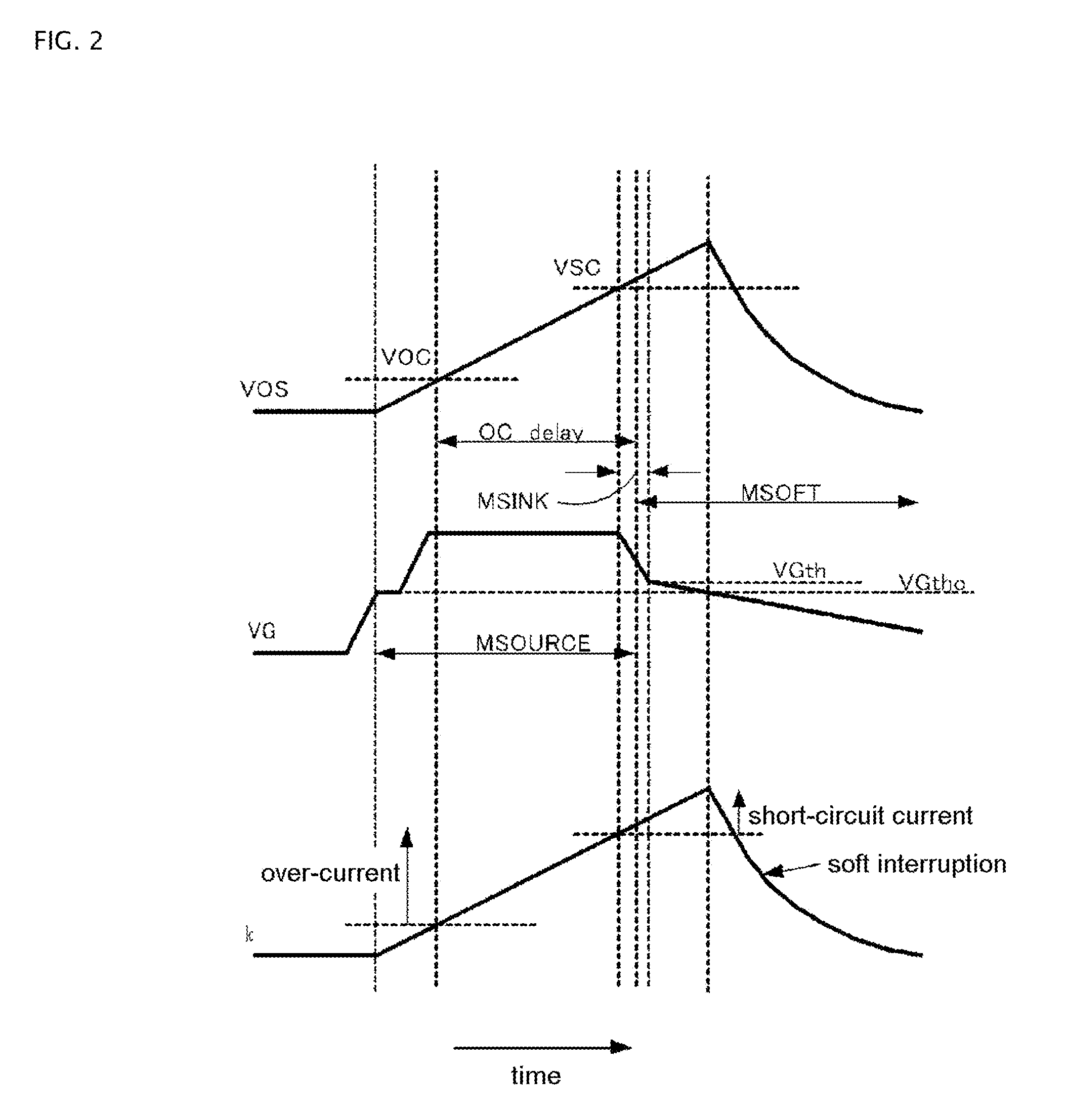
[0081]FIG. 5 shows operation waveforms in the gate driving circuit 300 of FIG. 4. The dotted lines in FIG. 5 show the waveforms in FIG....
PUM
 Abstract
Description
Claims
Application Information