Photoelectric conversion semiconductor layer, manufacturing method thereof, photoelectric conversion device, and solar cell

Inactive Publication Date: 2012-01-26
FUJIFILM CORP
View PDF1 Cites 19 Cited by
  • Summary
  • Abstract
  • Description
  • Claims
  • Application Information

AI Technical Summary

Benefits of technology

[0022]According to the present invention, a photoelectric conversion semiconductor layer capable of providing a potential gradient in the thickness direction, can be manufactured at a lower cost than a layer forme

Problems solved by technology

These methods, however, employ vacuum film forming, requiring a high manufacturing cost and a large equipment investment.
Even when a uniform layer appears to be formed, instead of an island-shaped layer, many voids are formed in the layer due to burning of an organic component, such as a dispersant, resulting in increased crystal defects and reduced light absorption, whereby a high efficient photoelectric conversion layer can not be provided.
Such method, however, increases the

Method used


Image

  • Photoelectric conversion semiconductor layer, manufacturing method thereof, photoelectric conversion device, and solar cell
  • Photoelectric conversion semiconductor layer, manufacturing method thereof, photoelectric conversion device, and solar cell
  • Photoelectric conversion semiconductor layer, manufacturing method thereof, photoelectric conversion device, and solar cell

Examples


example 1-1

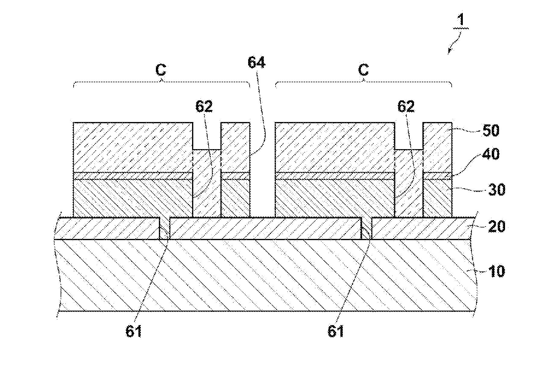
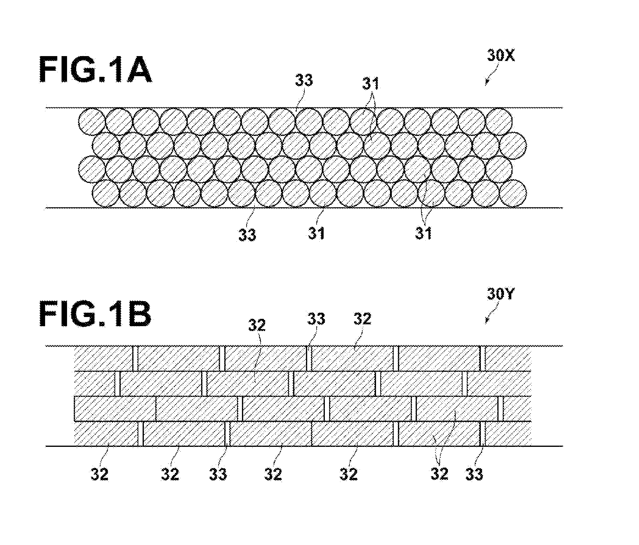
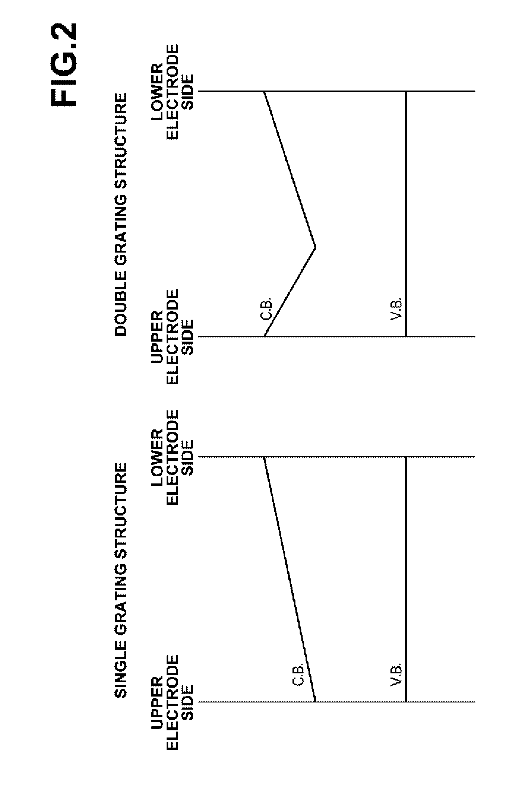
[0174]A Mo lower electrode (rear electrode) was formed on a soda lime glass by RF sputtering. The thickness of the lower electrode was 1.0 μm. Next, a coating material dispersed with spherical particles P3 was coated on the substrate having the lower electrode formed thereon to provide a single layer of spherical particles P3 (Ga: 8.8 at %), and a coating material dispersed with spherical particles P2 was coated on the layer of spherical particles P3 to provide a single layer of spherical particles P2 (Ga: 6.5 at %). The dispersion medium was removed by dissolving in toluene and heat drying at 180° C. for 60 minutes. This yielded a CIGS photoelectric conversion layer of two particle layers having a single grating structure.

[0175]Next, a semiconductor film having a laminated structure was formed as a buffer layer. First, a CdS film was deposited by chemical deposition with a thickness of about 50 nm. The chemical deposition was performed by heating an aqueous solution containing nitr...

example 1-2

[0177]A photoelectric conversion device of the present invention was obtained in the same manner as in Example 1-1 except that the process for preparing the photoelectric conversion layer was changed as follows. A coating material dispersed with spherical particles P3 was coated on the substrate having the lower electrode formed thereon to provide a single layer of spherical particles P3 (Ga: 8.8 at %), then a coating material dispersed with spherical particles P2 was coated on the layer of spherical particles P3 to provide a single layer of spherical particles P2 (Ga: 6.5 at %), a coating material dispersed with spherical particles P1 was coated on the layer of spherical particles P2 to provide a single layer of spherical particles P1 (Ga: 4.3 at %), and a coating material dispersed with spherical particles P2 was coated on the layer of spherical particles P1 to provide a single layer of spherical particles P2 (Ga: 0.3 at %). The dispersion medium was removed by dissolving in tolue...

example 1-3

[0178]A photoelectric conversion device of the present invention was obtained in the same manner as in Example 1-1 except that the process for preparing the photoelectric conversion layer was changed as follows. A coating material dispersed with spherical particles P6 was coated on the substrate having the lower electrode formed thereon to provide a single layer of spherical particles P6 (Ag: 6.4 at %), then a coating material dispersed with spherical particles P5 was coated on the layer of spherical particles P6 to provide a single layer of spherical particles P5 (Ag: 9.7 at %), a coating material dispersed with spherical particles P4 was coated on the layer of spherical particles P5 to provide a single layer of spherical particles P4 (Ag: 12.9 at %), a coating material dispersed with spherical particles P5 was coated on the layer of spherical particles P4 to provide a single layer of spherical particles P5 (Ag: 9.7 at %). The dispersion medium was removed by dissolving in toluene ...


PUM

PropertyMeasurementUnit
Temperatureaaaaaaaaaa
Fractionaaaaaaaaaa
Fractionaaaaaaaaaa

Abstract

A photoelectric conversion semiconductor layer is provided which is capable of providing a potential gradient in the thickness direction, can be manufactured at a lower cost than a layer formed by vacuum film forming, and capable of providing high photoelectric conversion efficiency. The photoelectric conversion semiconductor layer is a layer that generates a current by absorbing light and is formed of a particle layer in which a plurality of particles is disposed in plane and thickness directions. Preferably, the photoelectric conversion semiconductor layer includes, as the plurality of particles, a plurality of types of particles having different band-gaps, and the potential in the thickness direction of the layer is distributed.

Description

TECHNICAL FIELD[0001]The present invention relates to a photoelectric conversion semiconductor layer and a manufacturing method thereof, a photoelectric conversion device using the same, and a solar cell.BACKGROUND ART[0002]Photoelectric conversion devices, having a laminated structure in which a lower electrode (rear electrode), a photoelectric conversion semiconductor layer that generates a current by absorbing light, and an upper electrode are stacked, are used in various applications, such as solar cells and the like. Most of the conventional solar cells are Si-based cells using bulk monocrystalline Si, polycrystalline Si, or thin film amorphous Si. Recently, however, research and development of compound semiconductor-based solar cells that do not depend on Si has been carried out. Two types of compound semiconductor-based solar cells are known, one of which is a bulk system, such as GaAs system and the like, and the other of which is a thin film system, such as CIS (Cu—In—Se) s...

Claims


Application Information

Patent Timeline
IPC IPC(8): H01L31/0352H01L31/18H01L31/06H01L31/065H01L31/0749
CPCC23C18/1266C23C26/00C23C30/00C25D11/04C25D11/18C23C28/048H01L31/0749H01L31/1852Y02E10/541Y02E10/544H01L31/0322Y02P70/50H01L31/04H01L31/042H01L31/18
Inventor SATOU, TADANOBUKIKUCHI, MAKOTO
Owner FUJIFILM CORP
Why Eureka
Try Eureka