Memory control device, semiconductor memory device, memory system, and memory control method

a memory control device and memory control technology, applied in the security field, can solve the problems of deteriorating data processing rate, deteriorating data transfer efficiency, and difficult analysis of the specification of an operation performed between the external apparatus and the memory core, so as to improve data security, and increase the strength of encryption

Active Publication Date: 2012-01-26
MEGACHIPS
View PDF6 Cites 4 Cited by
  • Summary
  • Abstract
  • Description
  • Claims
  • Application Information

AI Technical Summary

Benefits of technology

[0006]For a further improvement of data security in a conventional memory system, it is conceivable to further increase the strength of encryption. However, increasing the strength of encryption may cause adverse effects such as a deterioration in the data processing rate and a deterioration in the data transfer efficiency. Therefore, a technique for improving data security by a method other than encryption is demanded.

Problems solved by technology

However, increasing the strength of encryption may cause adverse effects such as a deterioration in the data processing rate and a deterioration in the data transfer efficiency.
This makes it difficult to analyze a specification of an operation performed between the external apparatus and the memory core.

Method used


Image

  • Memory control device, semiconductor memory device, memory system, and memory control method
  • Memory control device, semiconductor memory device, memory system, and memory control method
  • Memory control device, semiconductor memory device, memory system, and memory control method

Examples


first embodiment

1. First Embodiment

[0030]

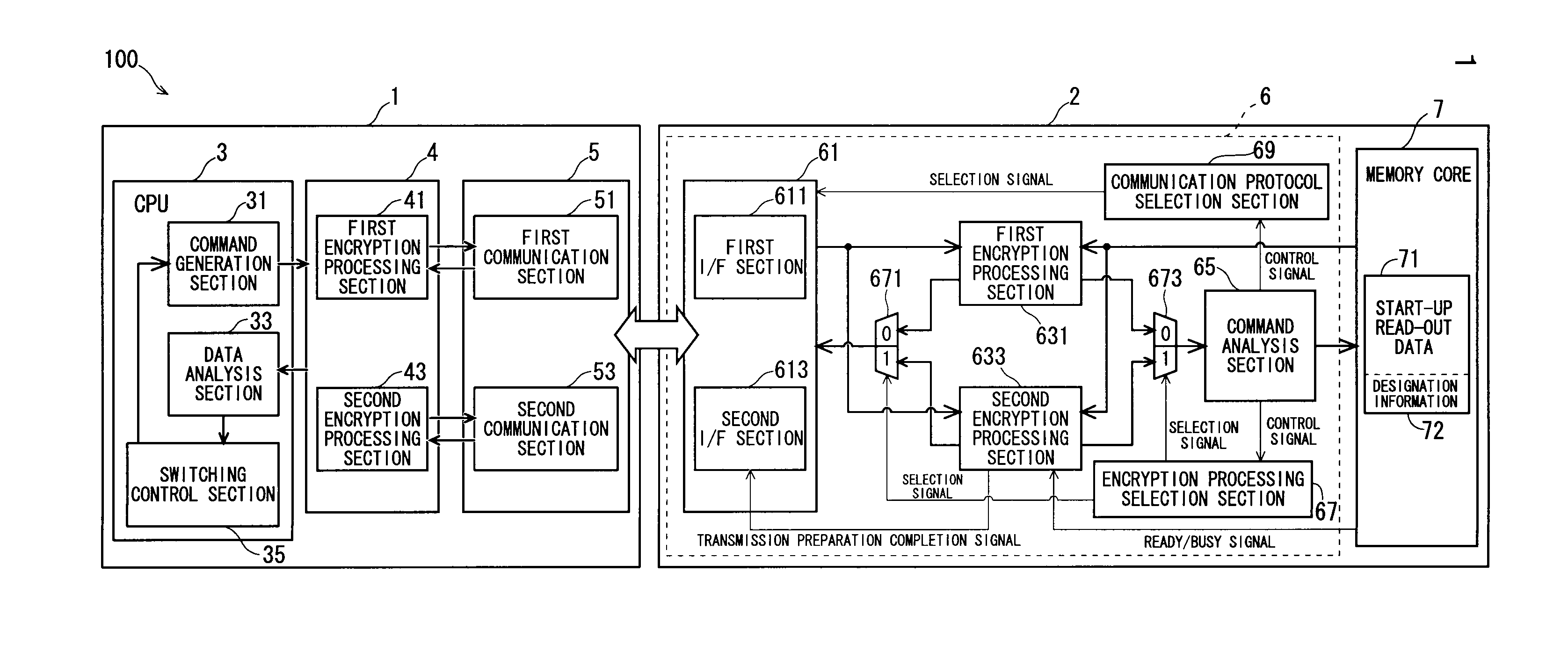
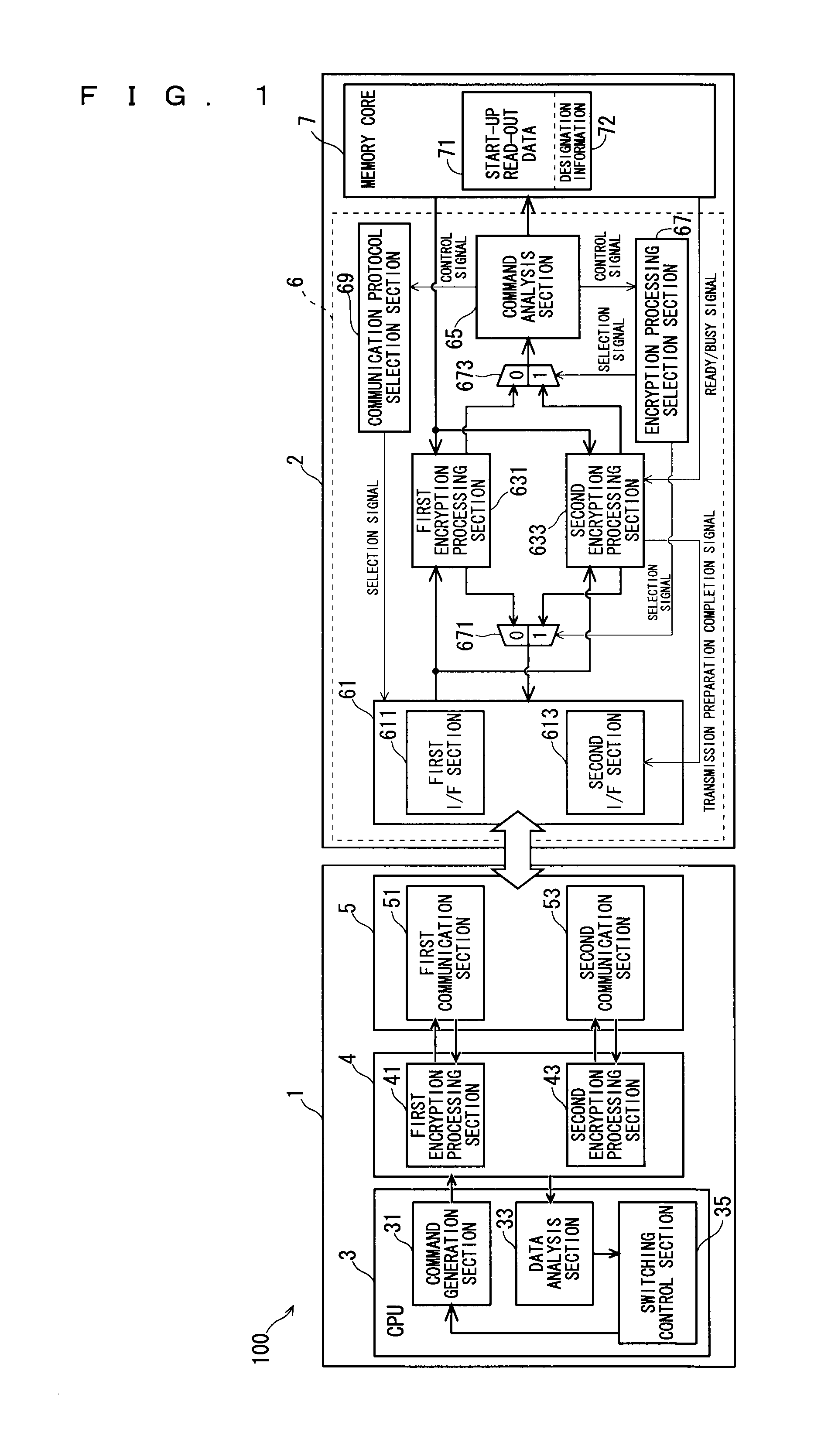
[0031]FIG. 1 is a block diagram showing a memory system 100 according to a first embodiment of the present invention. The memory system 100 according to the present invention includes an information processing apparatus 1 and a non-volatile semiconductor memory device (and more specifically, a ROM, a flash memory, or the like) 2 removably mounted to the information processing apparatus 1. The semiconductor memory device 2 stores therein, for example, a program and various content data, such as video data, image data, and music data, that are to be protected from unauthorized data reading. Although the information processing apparatus 1 is a general purpose apparatus, it may be an apparatus (such as a PDA and a mobile phone) dedicated to a special application.

[0032]1>

[0033]The information processing apparatus 1 includes a CPU 3, an encryption processing section 4, and a communication section 5. The information processing apparatus 1 has ordinary computer comp...

second embodiment

2. Second Embodiment

[0104]In the memory system 100 according to the first embodiment, the switching of the communication protocol is implemented by the information processing apparatus 1 recognizing the designation information 72 stored in the memory core 7. However, a method for switching the communication protocol is not limited thereto.

[0105]

[0106]FIG. 6 is a block diagram showing a memory system 100a according to a second embodiment. In a description of this embodiment, elements having the same functions as those of the first embodiment are denoted by the identical reference numerals, respectively, and descriptions thereof are omitted.

[0107]An information processing apparatus 1a of this embodiment includes a random number generation section 8 that generates a true or pseudo binary random number. Based on the binary random number generated by the random number generation section 8, a switching control section 35a that is implemented by an operation of a CPU 3a determines a commun...

third embodiment

3. Third Embodiment

[0117]Although in the above-described embodiment, an encryption processing section to be used for a particular communication protocol is fixed, a combination of the communication protocol and the encryption processing section is not limited to the fixed one.

[0118]FIG. 8 is a block diagram showing a memory system 100b according to a third embodiment. A CPU 3b included in an information processing apparatus 1b inputs a selection signal for selecting an element that performs encryption processing and communication to an encryption processing section 4a and a communication section 5a.

[0119]Based on a binary random number generated by the random number generation section 8, a switching control section 35b determines a communication protocol to be used in a memory system 100b, and also determines an encryption algorithm for encrypting a command and data to be communicated between the information processing apparatus I and the semiconductor memory device 2.

[0120]The com...


PUM


Abstract

A technique for improving data security is provided. To be specific, in a memory system including an information processing apparatus and a semiconductor memory device, the semiconductor memory device has an interface section that transmits, to the information processing apparatus, data read out from a memory core according to a plurality of communication protocols having different signal transmission/reception methods. Based on a switch command inputted from the information processing apparatus, a communication protocol selection section inputs, to the interface section, a selection signal for selecting a particular communication protocol from the plurality of communication protocols.

Description

TECHNICAL FIELD[0001]The present invention relates to a security technology for suppressing an unauthorized access to a memory core.BACKGROUND ART[0002]Conventionally, a memory system including an information processing apparatus and a semiconductor memory storing data therein is known. For example, a memory system is built with a computer serving as the information processing apparatus, a flash memory, and the like.[0003]In a conventional memory system, a semiconductor memory device employs some kind of a security function in order to prevent unauthorized copying of data by an unauthorized user or the like (for example, Patent Document 1).[0004]The Patent Document 1 discloses a technique in which address information inputted to a semiconductor memory device or data outputted from the semiconductor memory device is encrypted by a logic circuit to thereby protect the confidentiality of data.PRIOR-ART DOCUMENTSPatent Documents [0005]Patent Document 1: Japanese Patent Application Laid-...

Claims


Application Information

Patent Timeline
Patent Type & Authority Applications(United States)
IPC IPC(8): G06F12/14G06F21/60G06F21/62G06F21/72G06F21/75G06F21/78G06F21/86
CPCG06F2221/2105G06F21/72
Inventor SUGAHARA, TAKAHIKOFURUICHI, TETSUOYAMAGUCHI, IKUOOSHIKIRI, TAKASHI
Owner MEGACHIPS
Why Eureka
Try Eureka