Semiconductor laser apparatus and optical apparatus

Inactive Publication Date: 2012-02-02
SANYO ELECTRIC CO LTD
View PDF8 Cites 9 Cited by
  • Summary
  • Abstract
  • Description
  • Claims
  • Application Information

AI Technical Summary

Benefits of technology

[0022]In the aforementioned structure further comprising the base portion, the fifth lead terminal preferably further has heat radiation portions extending outward from the base portion. According to this structure, heat generated from the first, second and third semiconductor laser devices can be efficiently radiated through the base and the heat radiation portions.
[0023]In this case, the heat radiation portions are preferably seamlessly connected to sides of the mounting portions in the second direction and the fourth direction. According to this structure, heat generated from the semiconductor laser devices can be easily radiated through a pair of the heat radiation portions connected to the both sides of the mounting portion in the second direction and the fourth direction.
[0024]In the aforementioned semiconductor laser apparatus according to the first aspect, each of the first semiconductor laser device, the second semiconductor laser device and the third semiconductor laser device preferably has an active layer on a side bonded onto the upper surface of the base. According to this structure, the semiconductor laser devices are mounted on the base in a junction-down system, and hence heat can be efficiently radiated from the semiconductor laser devices toward the base. Consequently, temperature characteristics and reliability of the semiconductor laser devices can be improved.
[0025]In the aforementioned semiconductor laser apparatus according to the first aspect, the one electrode of the second semiconductor laser device is preferably conn

Problems solved by technology

However, the photodetector is provided behind the central semiconductor laser device, and hence a laser beam emitted from the central semiconductor laser device f

Method used


Image

  • Semiconductor laser apparatus and optical apparatus
  • Semiconductor laser apparatus and optical apparatus
  • Semiconductor laser apparatus and optical apparatus

Examples


first embodiment

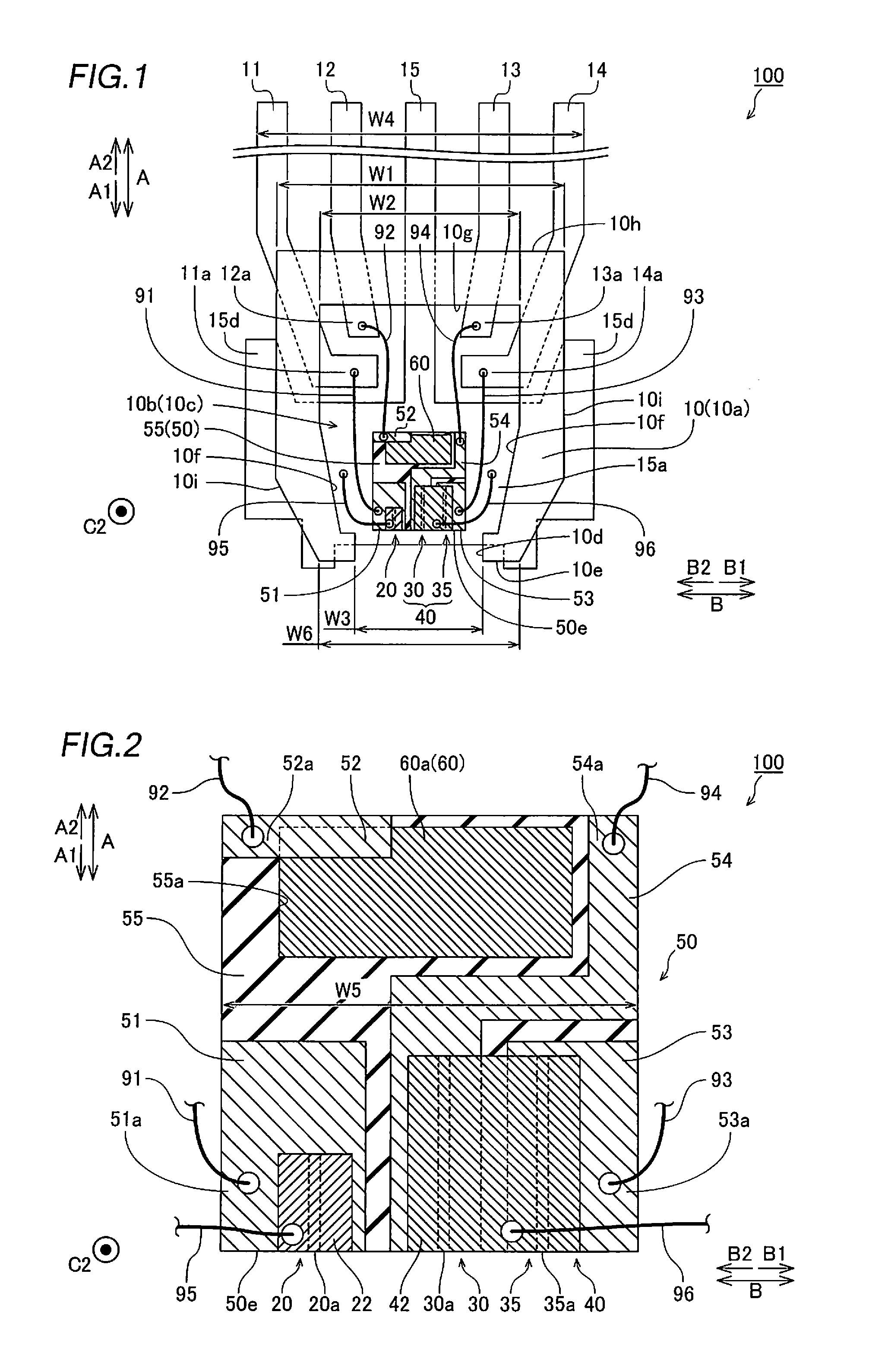
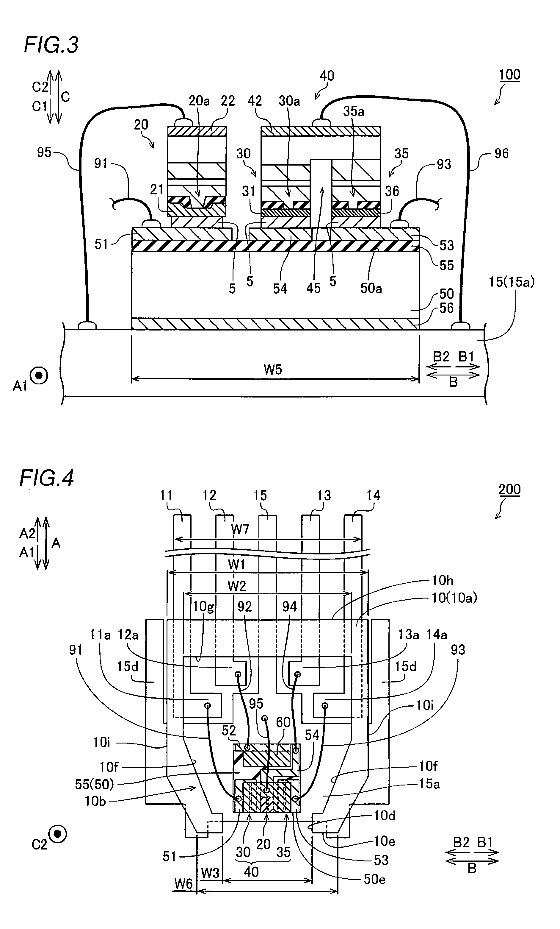
[0042]A structure of a three-wavelength semiconductor laser apparatus 100 according to a first embodiment of the present invention is now described with reference to FIGS. 1 to 3. The three-wavelength semiconductor laser apparatus 100 is an example of the “semiconductor laser apparatus” in the present invention.

[0043]A base portion 10 is made of a resin-molded insulator. The base portion 10 has a thickness of about 1.9 mm (in a direction C2). The base portion 10 has a width W6 in a width direction (in directions B1 and B2) at a front surface 10e on a front side (A1 side), which is an emitting side and a width W1 (W1>W6) on a rear side (A2 side). The base portion 10 has a recess portion 10b in an upper surface 10a, as shown in FIG. 1. A bottom surface of the recess portion 10b is arranged at a depth about half the thickness of the base portion 10. The recess portion 10b has an opening 10c with a width W2, which opens in the upper surface 10a (on a C2 side), and an opening 10d with a ...

second embodiment

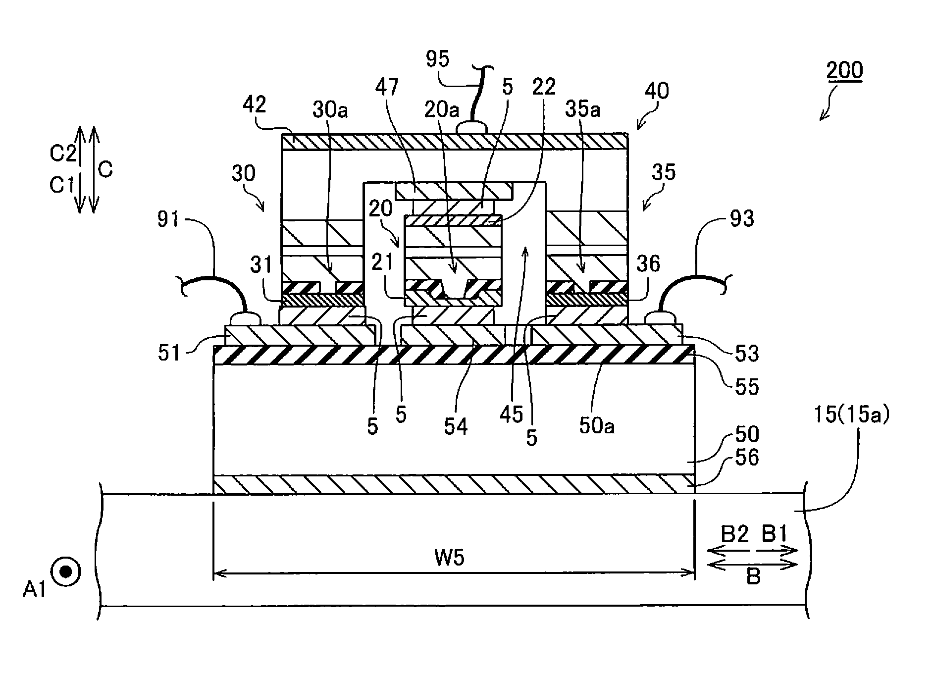
[0081]A three-wavelength semiconductor laser apparatus 200 according to a second embodiment of the present invention is now described. In this three-wavelength semiconductor laser apparatus 200, a blue-violet semiconductor laser device 20 is arranged on a substantially central portion of a submount 50 in a direction B, and a two-wavelength semiconductor laser device 40 is so arranged as to straddle an upside of the blue-violet semiconductor laser device 20 in the direction B, as shown in FIGS. 4 to 6. A red semiconductor laser device 30 and an infrared semiconductor laser device 35 constituting the two-wavelength semiconductor laser device 40 are arranged on B2 and B1 sides of the blue-violet semiconductor laser device 20, respectively. The three-wavelength semiconductor laser apparatus 200 is an example of the “semiconductor laser apparatus” in the present invention. The blue-violet semiconductor laser device 20, the red semiconductor laser device 30 and the infrared semiconductor ...

third embodiment

[0093]An optical pickup 300 according to a third embodiment of the present invention is now described. The optical pickup 300 is an example of the “optical apparatus” in the present invention.

[0094]The optical pickup 300 comprises the aforementioned three-wavelength semiconductor laser apparatus 100 according to the first embodiment, an optical system 320 adjusting laser beams emitted from the three-wavelength semiconductor laser apparatus 100 and a light detection portion 330 receiving the laser beams, as shown in FIG. 8.

[0095]The optical system 320 has a polarizing beam splitter (PBS) 321, a collimator lens 322, a beam expander 323, a λ / 4 plate 324, an objective lens 325, a cylindrical lens 326 and an optical axis correction device 327.

[0096]The PBS 321 totally transmits the laser beams emitted from the three-wavelength semiconductor laser apparatus 100, and totally reflects the laser beams fed back from an optical disc 335. The collimator lens 322 converts the laser beams emitted...


PUM


Abstract

In this semiconductor laser apparatus, a first wire-bonding portion is arranged at a position in a fourth direction from a first semiconductor laser device and in a first direction from a photodetector, and a second wire-bonding portion is arranged at a position in the fourth direction from the first semiconductor laser device and in a third direction from the first wire-bonding portion. A third wire-bonding portion is arranged at a position in a second direction from a third semiconductor laser device and in the first direction from the photodetector, and a fourth wire-bonding portion is arranged at a position in the second direction from the third semiconductor laser device and in the third direction from the third wire-bonding portion.

Description

CROSS-REFERENCE TO RELATED APPLICATION[0001]The priority application number JP2010-172376, Semiconductor Laser Apparatus and Optical Apparatus, Jul. 30, 2010, Masayuki Hata et al., upon which this patent application is based is hereby incorporated by reference.BACKGROUND OF THE INVENTION[0002]1. Field of the Invention[0003]The present invention relates to a semiconductor laser apparatus and an optical apparatus, and more particularly, it relates to a semiconductor laser apparatus and an optical apparatus each comprising a plurality of semiconductor laser devices.[0004]2. Description of the Background Art[0005]A semiconductor laser apparatus comprising a plurality of semiconductor laser devices is known in general, as disclosed in International Patent Laying-Open No. WO2005 / 039001, for example.[0006]International Patent Laying-Open No. WO2005 / 039001 discloses a two-beam semiconductor laser apparatus comprising a submount (base) and a two-wavelength semiconductor laser device fixed on...

Claims


Application Information

Patent Timeline
IPC IPC(8): H01S5/026H01S5/023
CPCH01S5/02236H01S5/0224H01S5/02256H01S5/4093H01S5/0683H01S5/4031H01S5/02276H01L2224/73265H01L2924/10155H01S5/02355H01S5/0234H01S5/023H01S5/0233H01S5/0235H01S5/02345
Inventor HATA, MASAYUKIYOSHIKAWA, HIDEKI
Owner SANYO ELECTRIC CO LTD
Why Eureka
Try Eureka