Dicing tape-integrated film for semiconductor back surface and method for producing the film, and method for producing semiconductor device

a technology of tape-integrated film and back surface, which is applied in the direction of film/foil adhesive, semiconductor/solid-state device testing/measurement, synthetic resin layered products, etc., can solve the problems of unsatisfactory visibility, increase in production cost and the like, and increase in the number of processing steps, etc., to achieve excellent peeling effect and suitable siz

Inactive Publication Date: 2012-02-02
NITTO DENKO CORP
View PDF10 Cites 36 Cited by
  • Summary
  • Abstract
  • Description
  • Claims
  • Application Information

AI Technical Summary

Benefits of technology

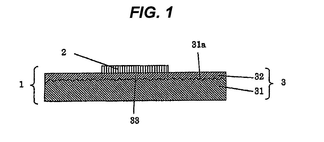
[0014]Preferably, the asperities-formed surface is an embossed surface. Embossing is easy as a treatment of base material and is excellent in easy peeling base materials from each other. In addition, the asperities formed on a surface through asperities-forming treatment by embossing thereon may have a suitable size, and therefore the close adhesiveness between the asperities-formed surface and the pressure-sensitive adhesive layer may be enhanced and, accordingly, the haze of the dicing tape can be thereby readily reduced.
[0015]Preferably, the base material and the pressure-sensitive adhesive layer has been laminated through thermal lamination. Heating in thermal lamination enhances the flexibility of the pressure-sensitive adhesive layer, and therefore the followability of the pressure-sensitive adhesive layer to the asperities of the asperities-formed surface may be thereby enhanced, and the gaps between the base material and the pressure-sensitive adhesive layer can be efficiently removed and the haze of the dicing tape can be further reduced.
[0016]Preferably, the thickness of the pressure-sensitive adhesive layer is from 10 μm to 50 μm. When the thickness of the pressure-sensitive adhesive layer falls within the above-mentioned range, then the close adhesiveness between the asperities-formed surface of the base material and the pressure-sensitive adhesive layer can be fully increased and the holding force of the semiconductor wafer being diced can be secured.
[0017]The present invention also provides a method for producing the dicing tape-integrated film for semiconductor back surface mentioned above (herein after may be referred to as “production method (i)), the method comprising: preparing a base material having an asperities-formed surface, laminating a...

Problems solved by technology

As a result, the number of the processing steps increases and the production cost and the like increase.
However, in conventional devices, the base material of the dicing tape often looks whitish and cloudy, and in such a cas...

Method used


Image

  • Dicing tape-integrated film for semiconductor back surface and method for producing the film, and method for producing semiconductor device
  • Dicing tape-integrated film for semiconductor back surface and method for producing the film, and method for producing semiconductor device
  • Dicing tape-integrated film for semiconductor back surface and method for producing the film, and method for producing semiconductor device

Examples


examples

[0148]The following will illustratively describe preferred Examples of the invention in detail. However, the invention is not limited to the following Examples unless it exceeds the gist thereof. Moreover, part in each example is a weight standard unless otherwise stated.

[0149]In a reaction vessel fitted with a cooling tube, a nitrogen inlet tube, a thermometer, and a stirring apparatus were placed 86.4 parts of 2-ethylhexyl acrylate (hereinafter referred to as “2EHA”), 13.6 parts of 2-hydroxyethyl acrylate (hereinafter referred to as “HEA”), 0.2 part of benzoyl peroxide, and 65 parts of toluene, and the whole was subjected to polymerization treatment in a nitrogen stream at 61° C. for 6 hours to give an acrylic polymer A.

[0150]To the acrylic polymer A was added 14.6 parts of 2-methacryloyloxyethyl isocyanate (hereinafter referred to as “MOI”), and the whole was subjected to addition reaction treatment in an air stream at 50° C. for 48 hours to give an acrylic polymer A′.

[0151]Then,...

examples 1 and 2

Preparation of Dicing Tape-Integrated Film for Semiconductor Back Surface

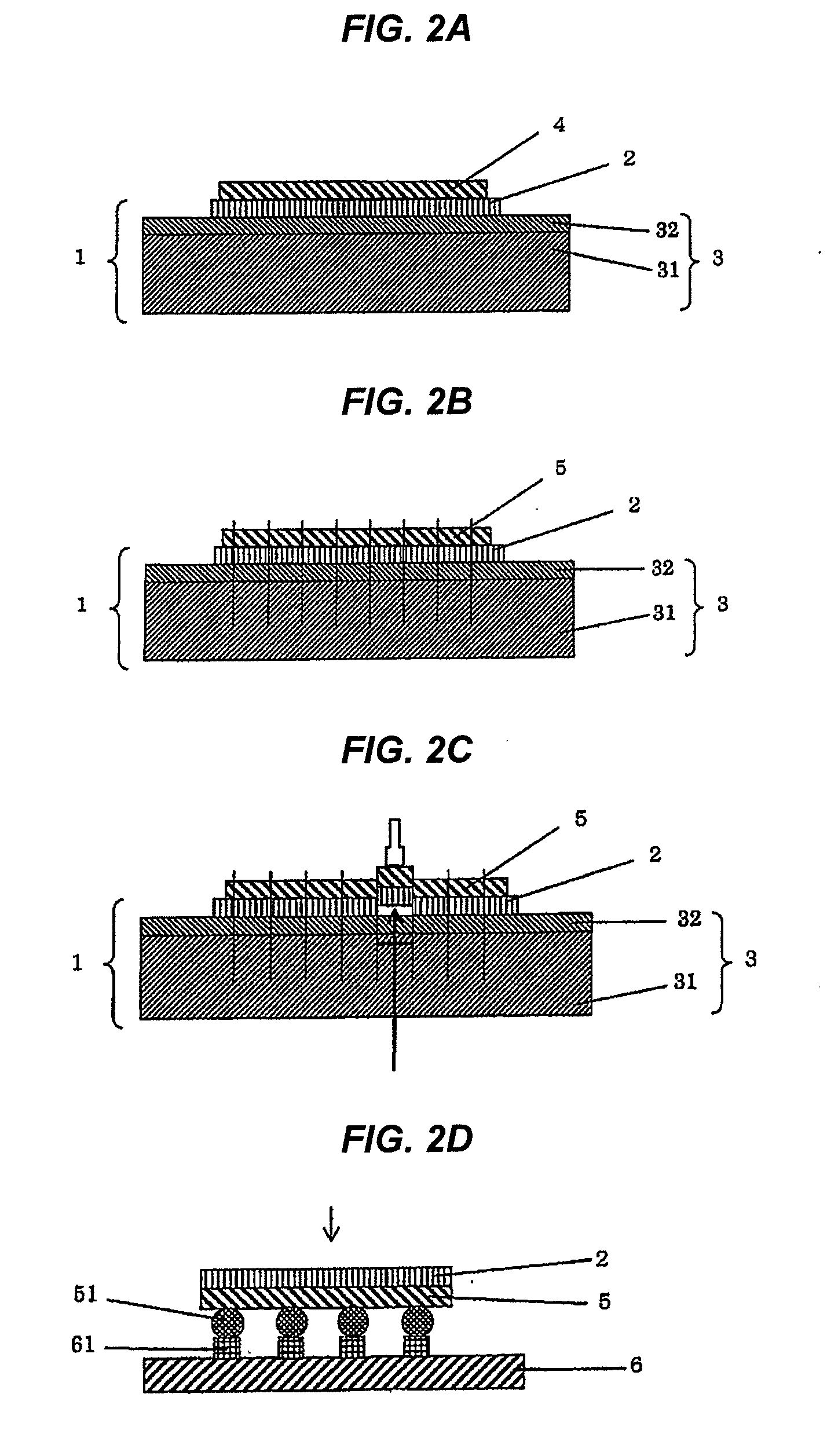
[0171]Using a hand roller, the obtained film A was attached to the dicing tape A or B, thereby preparing a dicing tape-integrated film for semiconductor back surface.

example 3

[0172]A dicing tape-integrated film for semiconductor back surface was prepared in the same manner as in Example 1, for which, however, the polyolefin film and the pressure-sensitive adhesive layer were laminated under the following thermal laminating conditions.

(Thermal Laminating Conditions)

[0173]Laminating Temperature: 40° C.

[0174]Laminating Pressure: 0.2 MPa


PUM

PropertyMeasurementUnit
Thicknessaaaaaaaaaa
Thicknessaaaaaaaaaa
Hazeaaaaaaaaaa

Abstract

The present invention relates to a dicing tape-integrated film for semiconductor back surface, which includes: a dicing tape including a base material having an asperities-formed surface, and a pressure-sensitive adhesive layer laminated on the base material, and a film for semiconductor back surface laminated on the pressure-sensitive adhesive layer of the dicing tape, in which the dicing tape has a haze of at most 45%.

Description

FIELD OF THE INVENTION[0001]The present invention relates to a dicing tape-integrated film for semiconductor back surface and a process for producing the film. The film for semiconductor back surface is used for protecting the back surface of a semiconductor element such as a semiconductor chip and for enhancing the strength thereof. The invention also relates to a method for producing a semiconductor device.BACKGROUND OF THE INVENTION[0002]Recently, thinning and miniaturization of a semiconductor device and its package have been increasingly demanded. Therefore, as the semiconductor device and its package, flip chip type semiconductor devices in which a semiconductor element such as a semiconductor chip is mounted (flip chip-connected) on a substrate by means of flip chip bonding have been widely utilized. In such flip chip connection, a semiconductor chip is fixed to a substrate in a form where the circuit face of the semiconductor chip is opposed to the electrode-formed face of t...

Claims


Application Information

Patent Timeline
IPC IPC(8): H01L21/78B32B3/00B32B37/00H01L21/66
CPCB32B7/12B32B27/08B32B2457/14Y10T428/24355H01L2924/014Y10T156/10H01L22/20B32B37/12B32B5/022B32B5/028B32B15/08B32B25/08B32B25/12B32B25/14B32B25/18B32B27/10B32B27/12B32B27/281B32B27/306B32B27/308B32B27/32B32B27/34B32B27/36B32B27/365B32B27/38B32B29/002B32B2250/44B32B2270/00B32B2274/00B32B2307/202B32B2307/302B32B2307/306B32B2307/514B32B2307/54B32B2307/732C09J7/20H01L21/6836H01L21/78H01L22/12H01L2924/35121B32B2307/414H01L24/81H01L2221/68327H01L2221/68386
Inventor TAKAMOTO, NAOHIDESHIGA, GOJIASAI, FUMITERU
Owner NITTO DENKO CORP
Why Eureka
Try Eureka