Detection device, light-receiving element array, semiconductor chip, method for manufacturing the same, and optical sensor apparatus

Inactive Publication Date: 2012-02-09
SUMITOMO ELECTRIC IND LTD
View PDF3 Cites 25 Cited by
  • Summary
  • Abstract
  • Description
  • Claims
  • Application Information

AI Technical Summary

Benefits of technology

[0047]The detection device etc. of the present invention are capable of preventing bump bonding failure and insulation failure, which are due to a difference in coefficient of thermal expansion, while securing a small size and low cost, thereby permitting transfer of high-quality pixel signals witho

Problems solved by technology

In general, a problem described below has occurred in thermal compression bonding between electrodes of a light-receiving element array and a read-out integrated circuit through bumps.
In forming bumps on a module substrate and in mounting on a mother substrate, the bumps are deformed due to a difference in coefficient of thermal expansion between silicon and a compound semiconductor, thereby causing bonding failure and insulation failure in the bumps.
In particular, in a two-dimensional arrangement of pixels, the pixels in an outer region are subjected to larger thermal stress, and thus the above-described problem significantly occurs.
However, for example, the cost of preparing, incorporating, and fixing the dummy substrate increases.
In addition, when an InP-based semiconductor is used on the sensor side, it is difficult to select a material having a proper coefficient of thermal expansion for the dummy substrate.
Further,

Method used


Image

  • Detection device, light-receiving element array, semiconductor chip, method for manufacturing the same, and optical sensor apparatus
  • Detection device, light-receiving element array, semiconductor chip, method for manufacturing the same, and optical sensor apparatus
  • Detection device, light-receiving element array, semiconductor chip, method for manufacturing the same, and optical sensor apparatus

Examples


first embodiment

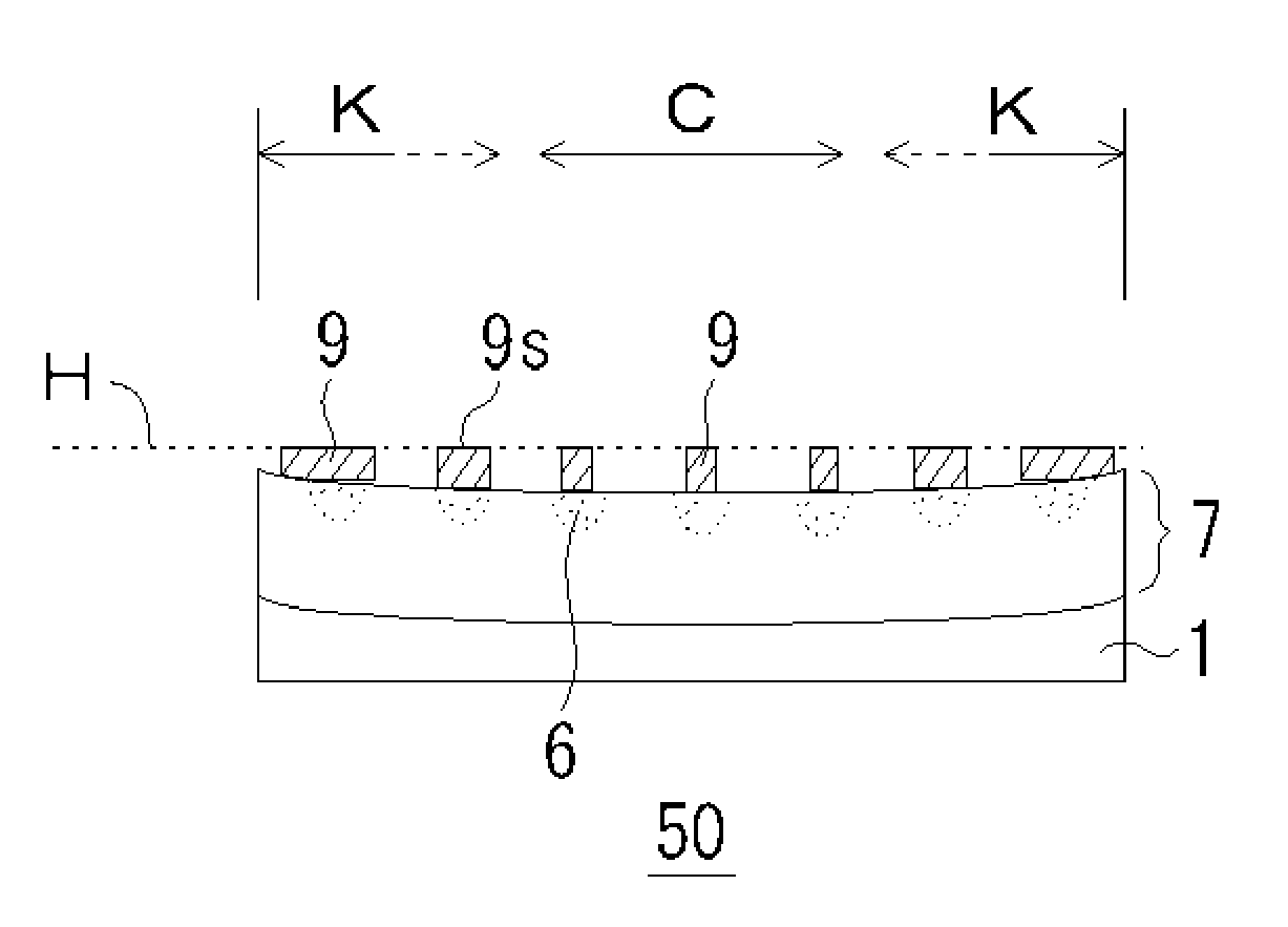
[0072]FIG. 1 is a drawing showing a light-receiving element array (sensor chip) 50 according to a first embodiment of the present invention. The light-receiving element array 50 includes an InP substrate 1 and an InP-based epitaxial stacked structure 7 formed on the InP substrate 1 and containing an absorption layer (not shown). In addition, p-type regions 6 are separately formed by selective diffusion of zinc (Zn) as p-type impurity from the surface of the InP epitaxial stacked structure 7. Each of the p-type regions serves as a core of a pixel. Further, a pixel electrode (p-side electrode) not shown is formed to make ohmic contact in each of the p-type regions 6, and bumps 9 are formed on the respective pixel electrodes. The characteristics of the light-receiving element array 50 according to this embodiment are as follows.

[0073](1) The epitaxial stacked structure 7 has an upwardly (outwardly) concaved surface.

[0074](2) The bumps 9 in a region K near the periphery have a larger di...

second embodiment

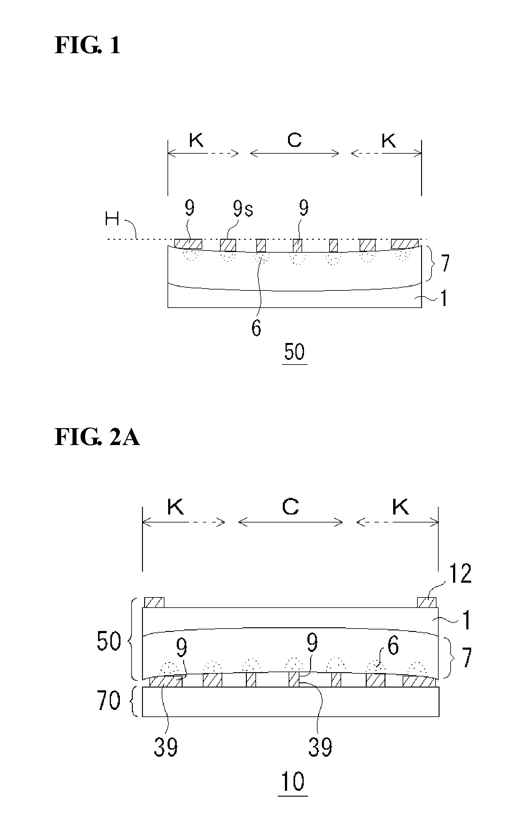
[0113]FIGS. 13A and 13B are drawings each showing a read-out integrated circuit 70 formed on silicon according to a second embodiment of the present invention. FIG. 13A is a drawing showing the case where the surface is entirely concavely warped in a bowl-like shape, and FIG. 13B is a drawing showing the case where the entire warp is eliminated to restore flatness. In both FIGS. 13A and 13B, the CMOS 70 includes a CMOS body 70a provided with read-out electrodes (not shown) and bumps 39 provided on the read-out electrodes.

[0114]In FIGS. 13A, the top surfaces 39s of the bumps 39 are arranged at the same height. On the other hand, in FIG. 13B, the height of the top surfaces 39s of the bumps 39 in the central region C are higher than the top surfaces 39s of the bumps 39 in the region K near the periphery (positioned away from the surface of the CMOS body 70a). This results from springback (restoration).

[0115]However, both cases are common in the point that the bumps 39 in the region K n...

third embodiment

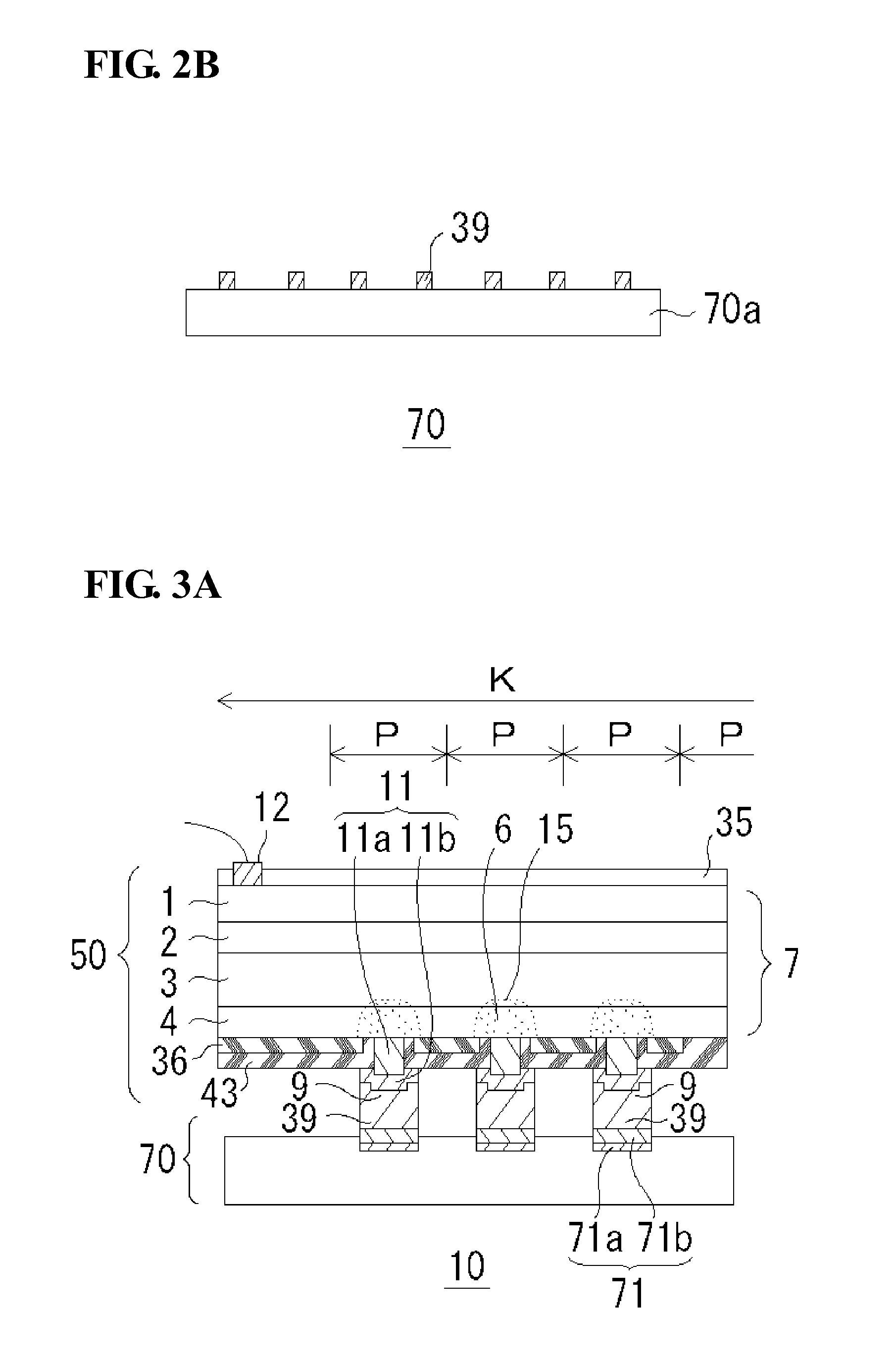
[0119]FIG. 16 is a drawing showing a detection device 10 according to a third embodiment of the present invention. This embodiment is characterized by using the light-receiving element array 50 of the first embodiment (refer to FIG. 1) and the CMOS 70 of the second embodiment (refer to FIG. 13A or 13B). That is, in the detection device 10 shown in FIG. 16, both the light-receiving element array 50 and the CMOS 70 have concaved surfaces which face each other. In addition, the bumps 9, 39 in the region K near the periphery have a larger diameter and a shorter length than the bonded bumps 9, 39 in the central region C. In more detail, the bonded bumps 9, 39 are increased in diameter and decreased in length from the center to the periphery with some variation, but strictly not in a linear manner. The bonded bumps 9, 39 have the above-described biased configuration. In particular, in this embodiment, the bumps 9 and 39 of both the light-receiving element array 50 and the CMOS 70 have the...


PUM


Abstract

A detection device includes a light-receiving element array and a read-out integrated circuit (CMOS), bumps of the light-receiving element array being bonded to bumps of the read-out integrated circuit, and at least one of the light-receiving element array and the read-out integrated circuit having a concaved surface which faces the other. The bonded bumps positioned in a region near the periphery of the arrangement region of the bonded bumps have a larger diameter and a lower height than those of the bumps positioned in a central region. Therefore, it is possible to prevent bonding failure and insulation failure in the bumps from occurring due to a difference in coefficient of thermal expansion, while securing a small size and low cost.

Description

BACKGROUND OF THE INVENTION[0001]1. Field of the Invention[0002]The present invention relates to a detection device including a light-receiving element array in which electrodes of pixels are arranged and a read-out integrated circuit in which read-out electrodes for reading out charges from the electrodes are arranged, the light-receiving element array and the read-out integrated circuit being bonded to each other, a light-receiving element array, a semiconductor chip, and an optical sensor apparatus, and methods for manufacturing the detection device, the light-receiving element array, and the read-out integrated circuit.[0003]2. Description of the Related Art[0004]Since the near-infrared region corresponds to an absorption spectral region related to living bodies of plants and animals and environments, near-infrared detectors using Group III-V compound semiconductors in absorption layers are actively developed. As the detectors, read-out integrated circuits (ROIC) including compl...

Claims


Application Information

Patent Timeline
IPC IPC(8): H01L31/0352H01L31/18H01L23/485B82Y20/00
CPCH01L24/11H01L27/1469H01L24/14H01L24/742H01L24/75H01L24/81H01L27/14634H01L27/14636H01L27/14694H01L2224/1184H01L2224/119H01L2224/13109H01L2224/13111H01L2224/1403H01L2224/75304H01L2224/759H01L2224/75983H01L2224/81201H01L2224/81815H01L2924/0103H01L2924/01049H01L2924/01051H01L2924/01079H01L2924/10155H01L2924/01005H01L2924/01006H01L2924/01019H01L2924/01023H01L2924/01033H01L2924/01078H01L24/13H01L2924/351H01L2924/12036H01L2924/14H01L2924/3511H01L2924/00
Inventor NAGAI, YOUICHIMORI, HIROKI
Owner SUMITOMO ELECTRIC IND LTD
Why Eureka
Try Eureka