Semiconductor device and method for driving semiconductor device

a semiconductor device and semiconductor technology, applied in semiconductor devices, digital storage, instruments, etc., can solve the problems of long time-consuming storage of semiconductor devices, achieve the effect of reducing power consumption, storing data for an extremely long time, and avoiding the frequency of refresh operations

Inactive Publication Date: 2012-02-09
SEMICON ENERGY LAB CO LTD
View PDF6 Cites 13 Cited by
  • Summary
  • Abstract
  • Description
  • Claims
  • Application Information

AI Technical Summary

Benefits of technology

[0025]Since the off-state current of a transistor including an oxide semiconductor is extremely small, stored data can be held for an extremely long time by using the transistor. In other words, power consumption can be adequately reduced because a refresh operation becomes unnecessary or the frequency of refresh operations can be extremely low. Moreover, stored data can be held for a long time even when power is not supplied (note that the potential is preferably fixed).
[0026]Further, a semiconductor device according to an embodiment of the disclosed invention does not need a high voltage for writing of data and there is no problem of deterioration of elements. For example, unlike a conventional non-volatile memory, it is not necessary to inject and extract electrons into and from a floating gate, and thus, a problem such as deterioration of a gate insulating layer does not occur at all. In other words, the semiconductor device according to an embodiment of the disclosed invention does not have a limitation on the number of times of writing operations which is a problem in a conventional non-volatile memory, and reliability thereof is drastically improved. Furthermore, data is written depending on an on state and an off state of a transistor, whereby a high-speed operation can be easily realized. In addition, there is no need of an operation for erasing data.
[0027]Since a transistor including a material other than an oxide semiconductor can operate at sufficiently high speed, a semiconductor device can perform an operation (e.g., reading data) at sufficiently high speed by combining such a transistor with a transistor including an oxide semiconductor. Further, with the use of a transistor including a material other than an oxide semiconductor, a variety of circuits (such as a logic circuit or a driver circuit) which are required to operate at high speed can be realized.

Problems solved by technology

When a semiconductor material which allows a sufficient reduction in off-state current of a transistor is used, the semiconductor device can hold data for a long time.

Method used


Image

  • Semiconductor device and method for driving semiconductor device
  • Semiconductor device and method for driving semiconductor device
  • Semiconductor device and method for driving semiconductor device

Examples


embodiment 1

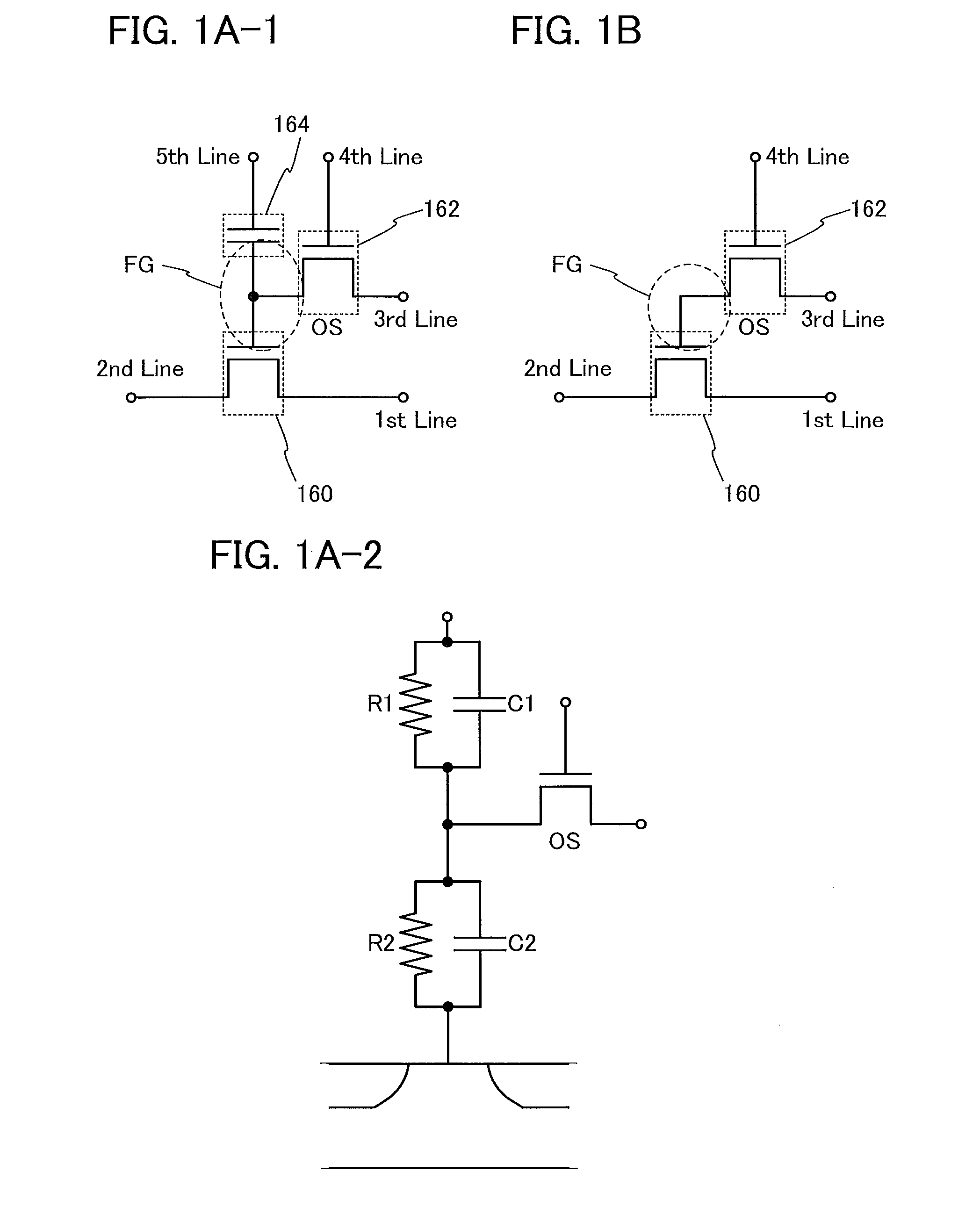
[0058]In this embodiment, a basic circuit structure and operation of a semiconductor device according to an embodiment of the disclosed invention will be described with reference to FIGS. 1A-1, 1A-2, and 1B and FIG. 2. Note that in each of circuit diagrams, in some cases, “OS” is written beside a transistor in order to indicate that the transistor includes an oxide semiconductor.

1>

[0059]First, the most basic circuit structure and its operation will be described with reference to FIGS. 1A-1, 1A-2, and 1B. In a semiconductor device illustrated in FIG. 1A-1, a first wiring (a first line) and a source electrode (or a drain electrode) of a transistor 160 are electrically connected to each other, and a second wiring (a second line) and the drain electrode (or the source electrode) of the transistor 160 are electrically connected to each other. In addition, a third wiring (a third line) and a source electrode (or a drain electrode) of a transistor 162 are electrically connected to each oth...

embodiment 2

[0120]In this embodiment, a structure and a manufacturing method of a semiconductor device according to an embodiment of the disclosed invention will be described with reference to FIGS. 5A and 5B, FIGS. 6A to 6G, FIGS. 7A to 7E, FIGS. 8A to 8D, FIGS. 9A to 9D, and FIGS. 10A to 10C.

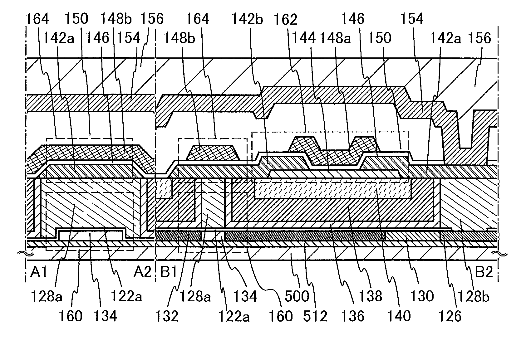
[0121]FIGS. 5A and 5B illustrate an example of a structure of a semiconductor device. FIG. 5A is a cross-sectional view of the semiconductor device, and FIG. 5B is a plan view of the semiconductor device. FIG. 5A corresponds to a cross section along line A1-A2 and line B1-B2 in FIG. 5B. The semiconductor device illustrated in FIGS. 5A and 5B includes a transistor 160 including a first semiconductor material in a lower portion, and a transistor 162 including a second semiconductor material in an upper portion. Here, the first semiconductor material and the second semiconductor material are preferably different materials. For example, a semiconductor material other than an oxide semiconductor can be used as...

embodiment 3

[0250]In this embodiment, the case where the semiconductor device described in any of the above embodiments is applied to electronic devices will be described with reference to FIGS. 11A to 11F. In this embodiment, the semiconductor device described in any of the above embodiments can be applied to electronic device such as computer, a mobile phone set (also referred to as a mobile phone or a mobile phone device), a personal digital assistant (including a portable game machine, an audio reproducing device, and the like), a camera such as a digital camera or a digital video camera, an electronic paper, and a television device (also referred to as a television or a television receiver).

[0251]FIG. 11A illustrates a laptop personal computer, which includes a housing 701, a housing 702, a display portion 703, a keyboard 704, and the like. The semiconductor device described in any of the above embodiments is provided in at least one of the housing 701 and the housing 702. Therefore, a lap...


PUM


Abstract

It is an object to provide a semiconductor device with a novel structure in which stored data can be held even when power is not supplied, and does not have a limitation on the number of writing operations. A semiconductor device includes a plurality of memory cells each including a transistor including a first semiconductor material, a transistor including a second semiconductor material that is different from the first semiconductor material, and a capacitor, and a potential switching circuit having a function of supplying a power supply potential to a source line in a writing period. Thus, power consumption of the semiconductor device can be sufficiently suppressed.

Description

BACKGROUND OF THE INVENTION[0001]1. Field of the Invention[0002]The disclosed invention relates to a semiconductor device including a semiconductor element and a method for driving the semiconductor device.[0003]2. Description of the Related Art[0004]Storage devices including semiconductor elements are broadly classified into two categories: a volatile device that loses stored data when power is not supplied, and a non-volatile device that holds stored data even when power is not supplied.[0005]A typical example of a volatile storage device is a DRAM (dynamic random access memory). A DRAM stores data in such a manner that a transistor included in a storage element is selected and electric charge is stored in a capacitor.[0006]When data is read from a DRAM, electric charge in a capacitor is lost owing to the above-described principle; thus, another writing operation is necessary whenever data is read out. Moreover, since leakage current (off-state current) flows between a source and ...

Claims


Application Information

Patent Timeline
Patent Type & Authority Applications(United States)
IPC IPC(8): G11C11/24H01L27/06H01L29/04
CPCG11C11/405G11C16/0408G11C16/02H10B99/00H10B12/00
Inventor INOUE, HIROKIKATO, KIYOSHIMATSUZAKI, TAKANORINAGATSUKA, SHUHEI
Owner SEMICON ENERGY LAB CO LTD
Why Eureka
Try Eureka