Method of Making an Organic Thin Film Transistor

a thin film transistor and organic technology, applied in the direction of transistors, semiconductor devices, electrical devices, etc., can solve problems such as curved domains

Inactive Publication Date: 2012-02-16
CAMBRIDGE DISPLAY TECH LTD
View PDF1 Cites 7 Cited by
  • Summary
  • Abstract
  • Description
  • Claims
  • Application Information

AI Technical Summary

Benefits of technology

[0031]In particular, the method of forming a thin film transistor comprising source and drain electrodes with a channel region therebetween, a gate electrode, a dielectric layer disposed between the source and drain electrodes and the gate electrode, and an organic semiconductor disposed in at least the channel region between the source and drain electrodes, said method comprising: seeding a surface outside the channel region with one or more sites for initiating crystallization (crystallization sites) prior to deposition of the organic semiconductor; depositing a solution of the organic semiconductor onto the seeded surface and over the channel region whereby the organic semiconductor begins forming a crystal domain at the or each of the crystallisation sites, the or each crystal domain growing from its crystallisation site across the channel region in a direction determined by an advancing surface evaporation front; and applying energy to control the direction and rate of movement of the surface evaporation front thereby controlling the direction and rate of growth of the or each crystal domain across the channel region from the one or more crystallization sites outside the channel region.
[0047]According to an alternative arrangement, the organic thin film transistor is a top-gate organic thin film transistor and the method comprises: forming the source and drain electrodes over the substrate, the source and drain electrodes being spaced apart with the channel region therebetween; seeding the surface outside the channel region with one or more crystallization sites; depositing the solution of the organic semiconductor onto the seeded surface and over the channel region; controlling the direction and rate of movement of the surface evaporation front thereby controlling the direction and rate of growth of the or each crystal domain across the channel region from the one or more crystallization sites outside the channel region; forming the dielectric layer over the organic semiconductor; and depositing the gate electrode over the dielectric layer.

Problems solved by technology

One disadvantage of this approach is that the resulting crystal domains will be curved requiring a corresponding alignment of the source and drain electrodes.

Method used


Image

  • Method of Making an Organic Thin Film Transistor
  • Method of Making an Organic Thin Film Transistor
  • Method of Making an Organic Thin Film Transistor

Examples


Embodiment Construction

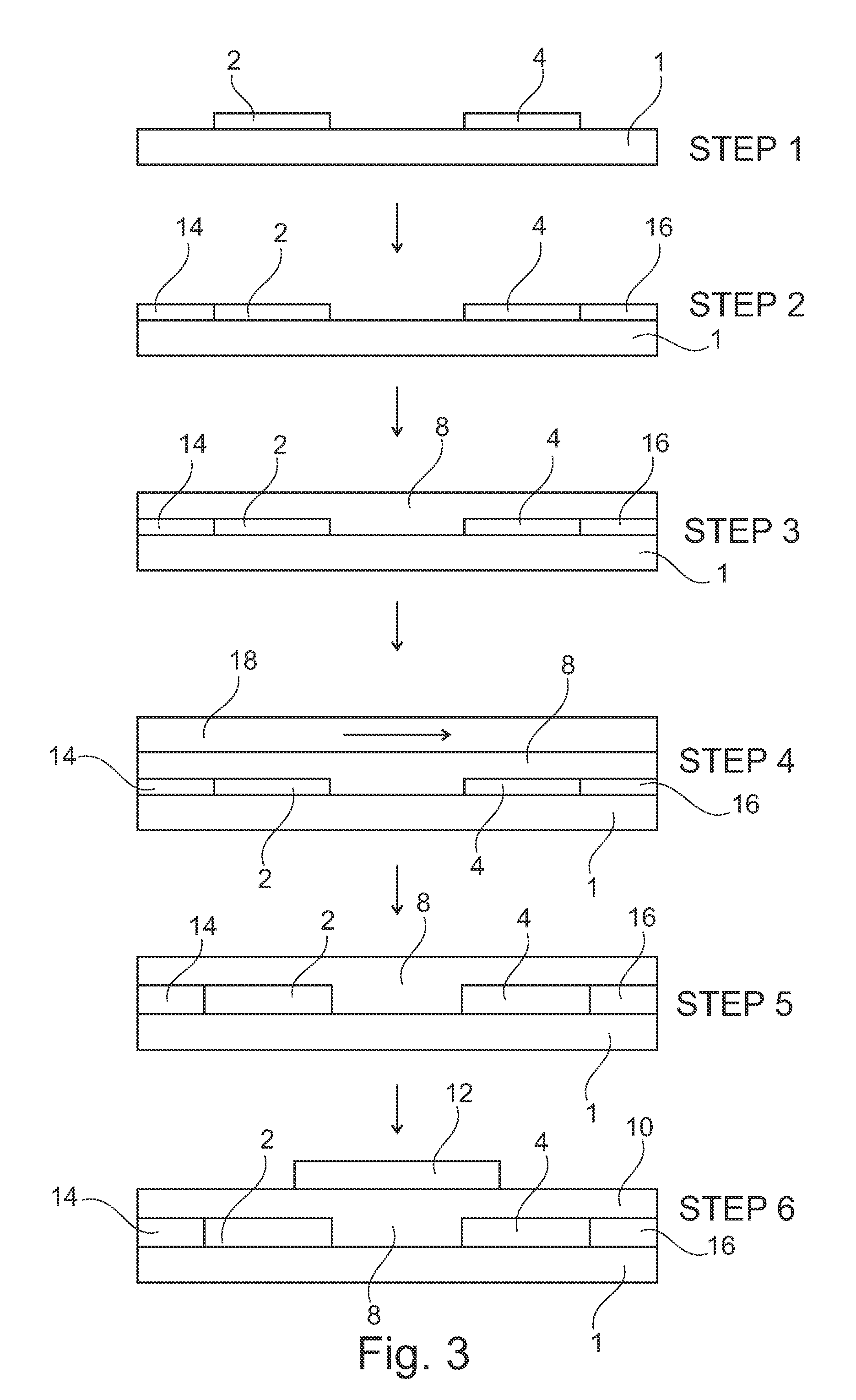
[0057]An example method of how the present technique may be carried out is shown schematically in FIG. 3.

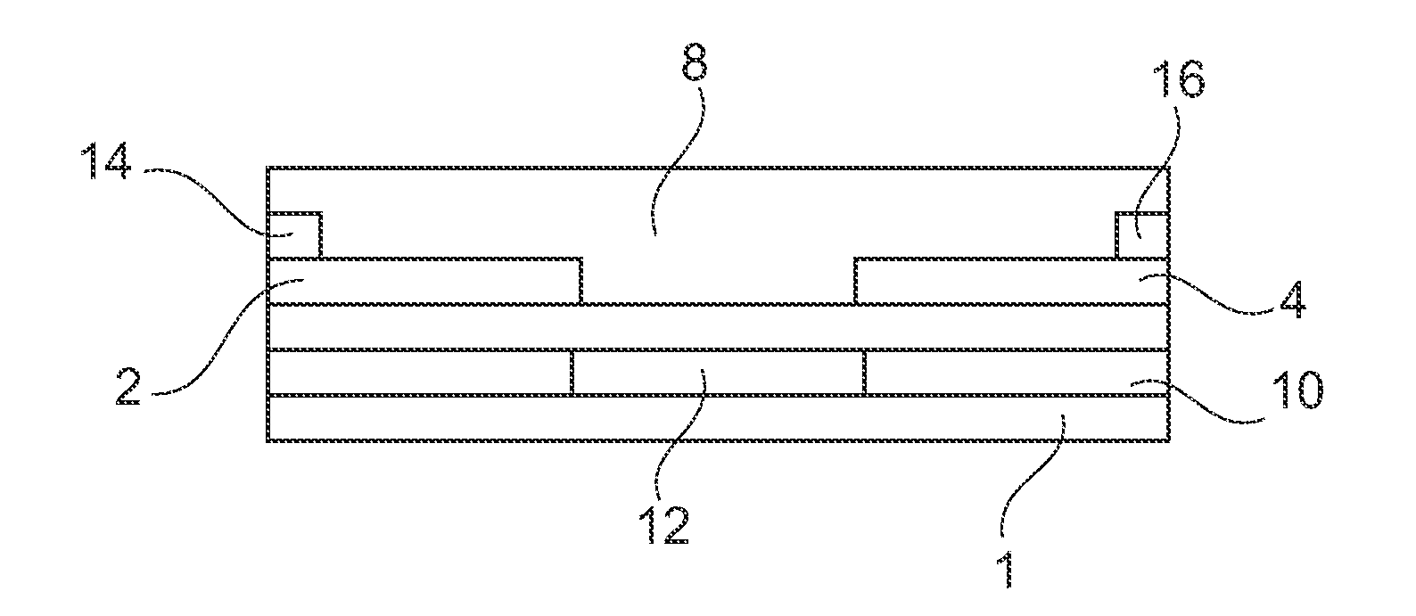
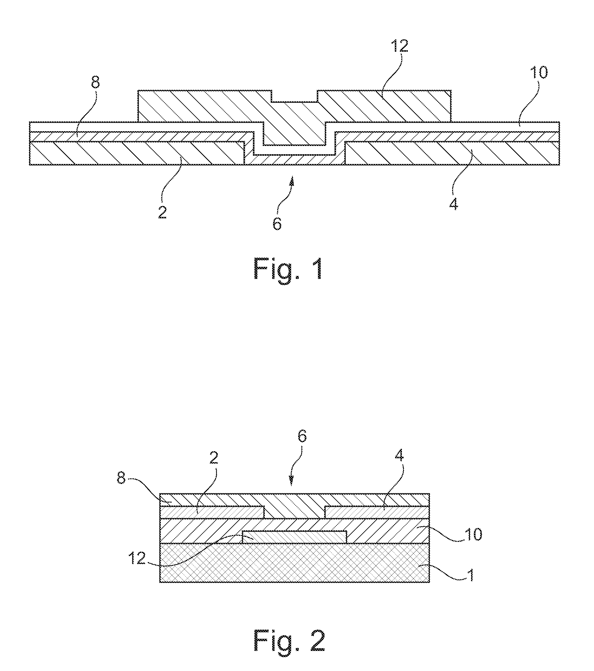
[0058]In step 1, a substrate 1 is initially prepared by formation of source and drain electrodes 2, 4 thereon.

[0059]In step 2, crystallisation sites 14, 16 are formed on the substrate 1 adjacent the source and drain electrodes 2, 4. The crystallisation sites 14, 16 may comprise a de-wetting material such as Teflon™.

[0060]In step 3, a solution of an organic semiconductor 8 is deposited. The organic semi-conductive material may be solution processable such that it can be deposited from solution by, for example, ink-jet printing. The organic semi-conductive material may comprise a small molecule organic semi-conductor, a polymer or a dendrimer. Many such semi-conductive materials are known in the art.

[0061]In step 4, while the solution of organic semiconductor 8 is still wet, a shearing substrate 18 is placed on the solution and dragged in a source-to-drain direction as indicated by...


PUM


Abstract

A method of forming an organic thin film transistor the method comprising:seeding a surface outside a channel region with one or more crystallization sites prior to deposition of the organic semiconductor;depositing a solution of the organic semiconductor onto the seeded surface and over the channel region whereby the organic semiconductor begins forming a crystal domain at the or each of the crystallization sites, the or each crystal domain growing from its crystallization site across the channel region in a direction determined by an advancing surface evaporation front; andapplying energy to control the direction and rate of movement of the surface evaporation front thereby controlling the direction and rate of growth of the or each crystal domain across the channel region from the one or more crystallization sites outside the channel region.

Description

FIELD OF INVENTION[0001]The present invention relates to organic thin film transistors and methods of making them.BACKGROUND OF THE INVENTION[0002]Transistors can be divided into two main types: bipolar junction transistors and field-effect transistors. Both types share a common structure comprising three electrodes with a semi-conductive material disposed therebetween in a channel region. The three electrodes of a bipolar junction transistor are known as the emitter, collector and base, whereas in a field-effect transistor the three electrodes are known as the source, drain and gate. Bipolar junction transistors may be described as current-operated devices as the current between the emitter and collector is controlled by the current flowing between the base and emitter. In contrast, field-effect transistors may be described as voltage-operated devices as the current flowing between source and drain is controlled by the voltage between the gate and the source.[0003]Transistors can a...

Claims


Application Information

Patent Timeline
Patent Type & Authority Applications(United States)
IPC IPC(8): H01L29/786H01L21/20
CPCH01L51/0012H10K71/191H10K71/12H10K10/462H10K71/15
Inventor KUGLER, THOMAS
Owner CAMBRIDGE DISPLAY TECH LTD
Why Eureka
Try Eureka