
Eureka
For R&D, Eureka makes reading and utilizing patents & technical documents easy.
Eureka AIR
Designed for self-driven R&D workflows. Generate viable solutions, solve complex R&D challenges, empower your innovation with AI.

Eureka Materials
Designed for material experts only. Revolutionize your material R&D, from search, analyze, to developing new materials.

TechResearch
Generate reliable direction feasibility study reports for your R&D in just a few steps.

TechSeek
Discover and master advanced knowledge NOW. Basics, ideas, possibilities, all at once.

TechMind
As an expert in R&D Theories, TechMind can generates customized viable solutions instantly.

TechRisk
Analyze your overall solution with one click, know your potential R&D risks in advance.

TechMonitor
Get weekly tech updates, stay abreast of the latest tech innovations and key insights.
Manufacturing method of semiconductor device
- Summary
- Abstract
- Description
- Claims
- Application Information
AI Technical Summary
Benefits of technology
Problems solved by technology
Method used
Image

Examples
embodiment 1
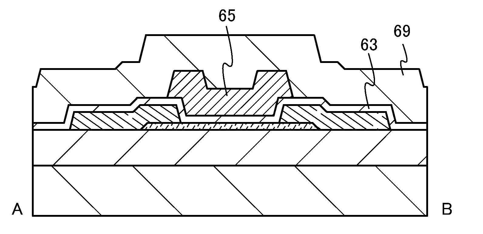
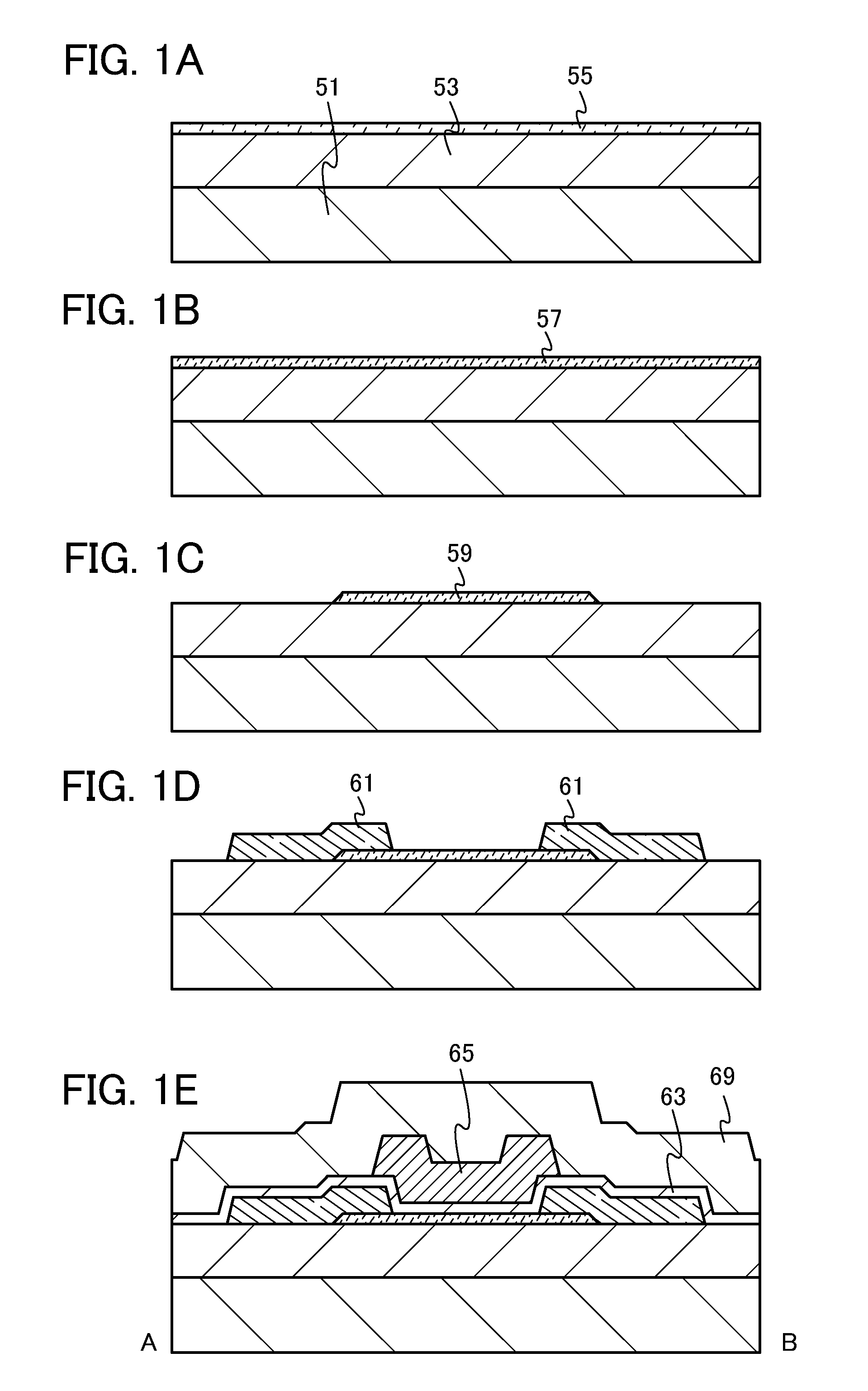
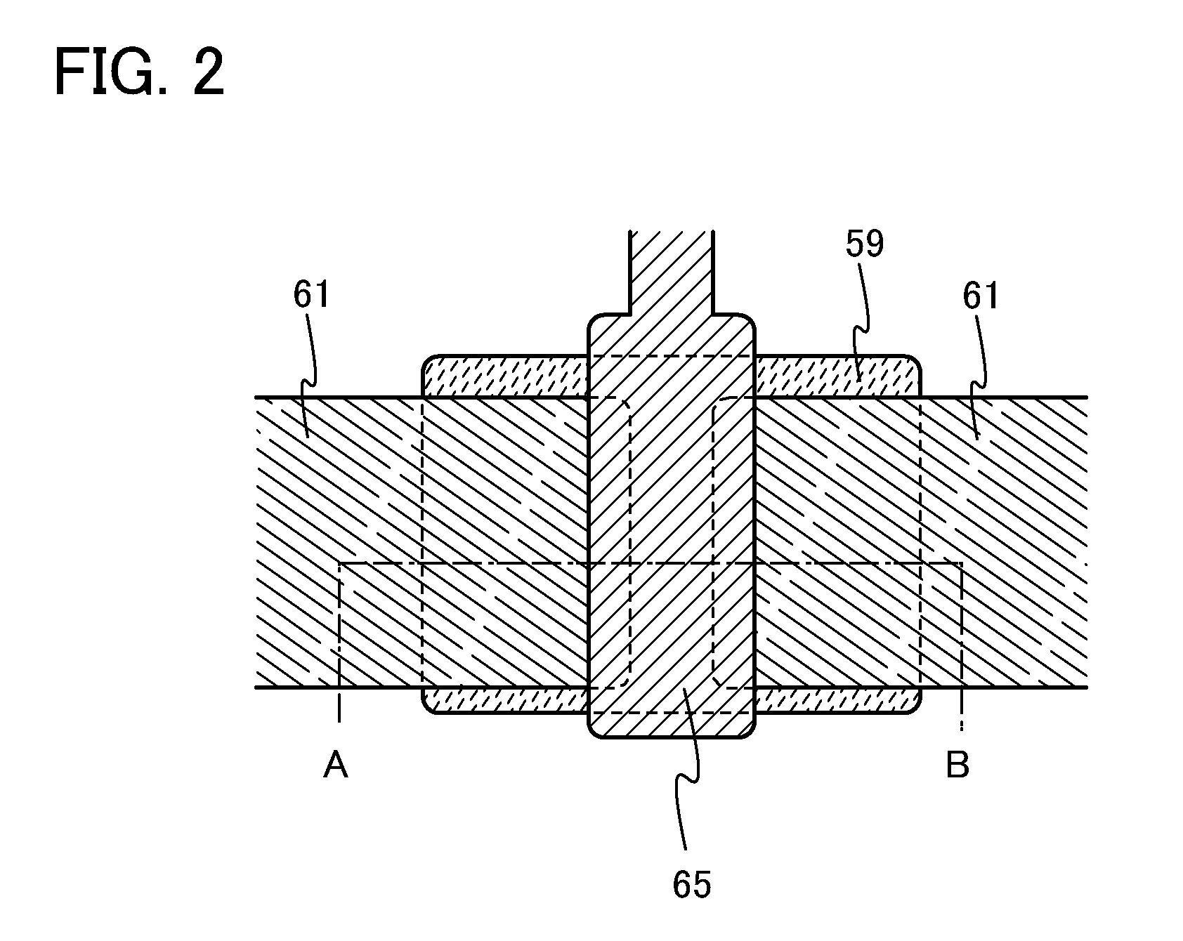
[0037]FIGS. 1A to 1E are cross-sectional views illustrating a manufacturing process of a transistor as one mode of a structure of a semiconductor device. The cross-sectional view taken along the dot-dash line A-B in FIG. 2 corresponds to FIG. 1E.
[0038]As illustrated in FIG. 1A, an oxide insulating film 53 is formed over a substrate 51, and an oxide semiconductor film 55 is formed over the oxide insulating film 53.
[0039]As the substrate 51, a glass substrate (also referred to as a “non-alkali glass substrate”), a quartz substrate, a ceramic substrate, a plastic substrate, or the like can be used as appropriate. Further, a flexible glass substrate or a flexible plastic substrate can be used as the substrate 51. As a plastic substrate, a substrate having low refractive index anisotropy is preferably used, and a polyether sulfone (PES) film, a polyimide film, a polyethylene naphthalate (PEN) film, a polyvinyl fluoride (PVF) film, a polyester film, a polycarbonate (PC) film, an acrylic r...
embodiment 2
[0088]In Embodiment 2, a manufacturing method of a transistor having a structure different from the transistor described in Embodiment 1 will be described with reference to FIGS. 3A to 3D, and FIG. 4. Embodiment 2 is different from Embodiment 1 in that a pair of electrodes is provided between an oxide insulating film and an oxide semiconductor film. Note that the cross-sectional view taken along the dot-dash line A-B in FIG. 4 corresponds to FIG. 3D.
[0089]As illustrated in FIG. 3A, the oxide insulating film 53 is formed over the substrate 51 as in Embodiment 1. A pair of electrodes 71 is formed over the oxide insulating film 53. An oxide semiconductor film 73 is formed over the pair of electrodes 71 and the oxide insulating film 53.
[0090]The pair of electrodes 71 can be formed as appropriate by using a material and by a formation method which are similar to those of the pair of electrodes 61 described in Embodiment 1.
[0091]The oxide semiconductor film 73 can be formed as appropriate...
embodiment 3
[0101]In Embodiment 3, a manufacturing method of a transistor where a contact resistance between an oxide semiconductor film and a pair of wirings can be decreased more than those of the transistors described in Embodiment 1 and Embodiment 2 will be described with reference to FIGS. 1A to 1E and FIGS. 5A to 5E.
[0102]As in Embodiment 1, in the steps illustrated in FIGS. 1A and 1B, the oxide semiconductor film 55 is formed over the oxide insulating film 53 and is heated to form the oxide semiconductor film 57 with the lowered hydrogen concentration and the reduced oxygen vacancies. Next, as illustrated in FIG. 5A, a buffer 84 having an n-type conductivity is formed over the oxide semiconductor film 57 with the lowered hydrogen concentration and the reduced oxygen vacancies.
[0103]For the buffer 84 having an n-type conductivity, a metal oxide selected from the group of indium oxide, indium tin oxide, indium zinc oxide, tin oxide, zinc oxide, and tin zinc oxide, or a material of the meta...
PUM
 Abstract
Description
Claims
Application Information
 - R&D Engineer
- R&D Manager
- IP Professional
- Industry Leading Data Capabilities
- Powerful AI technology
- Patent DNA Extraction
Browse by: Latest US Patents, China's latest patents, Technical Efficacy Thesaurus, Application Domain, Technology Topic, Popular Technical Reports.
© 2024 PatSnap. All rights reserved.Legal|Privacy policy|Modern Slavery Act Transparency Statement|Sitemap|About US| Contact US: help@patsnap.com