Ultra-thin body transistor and method for manufcturing the same

a transistor and ultra-thin body technology, applied in the field of ultra-thin body transistors and manufacturing methods, can solve the problems of limiting the further scaling down and performance improvement of devices, the complexity of ics has been advanced to an unimaginable level, and the effect of reducing the effect to the effective length of the channel, reducing the parasitic resistance, and reducing the effect of body region

Inactive Publication Date: 2012-02-23
INST OF MICROELECTRONICS CHINESE ACAD OF SCI
View PDF12 Cites 33 Cited by
  • Summary
  • Abstract
  • Description
  • Claims
  • Application Information

AI Technical Summary

Benefits of technology

[0023]In comparison with conventional technologies, the present invention has the following advantages:
[0024]1. The ultra-thin body transistor has a thinner body region, which decreases the effect to the effective length of channel caused by the lateral depletion region under drain reverse

Problems solved by technology

The performance and complexity of ICs have been advanced to an unimaginable level.
However, the body region of the MOS transistor is thick, which

Method used


Image

  • Ultra-thin body transistor and method for manufcturing the same
  • Ultra-thin body transistor and method for manufcturing the same
  • Ultra-thin body transistor and method for manufcturing the same

Examples


Embodiment Construction

[0030]The present invention will be described hereafter in detail with reference to embodiments, in conjunction with the accompanying drawings.

[0031]Embodiments to which the present invention is applied are described in detail below. However, the invention is not restricted to the embodiments described below.

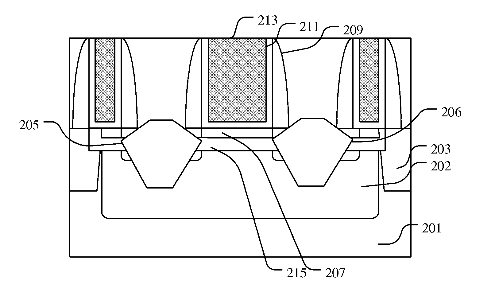
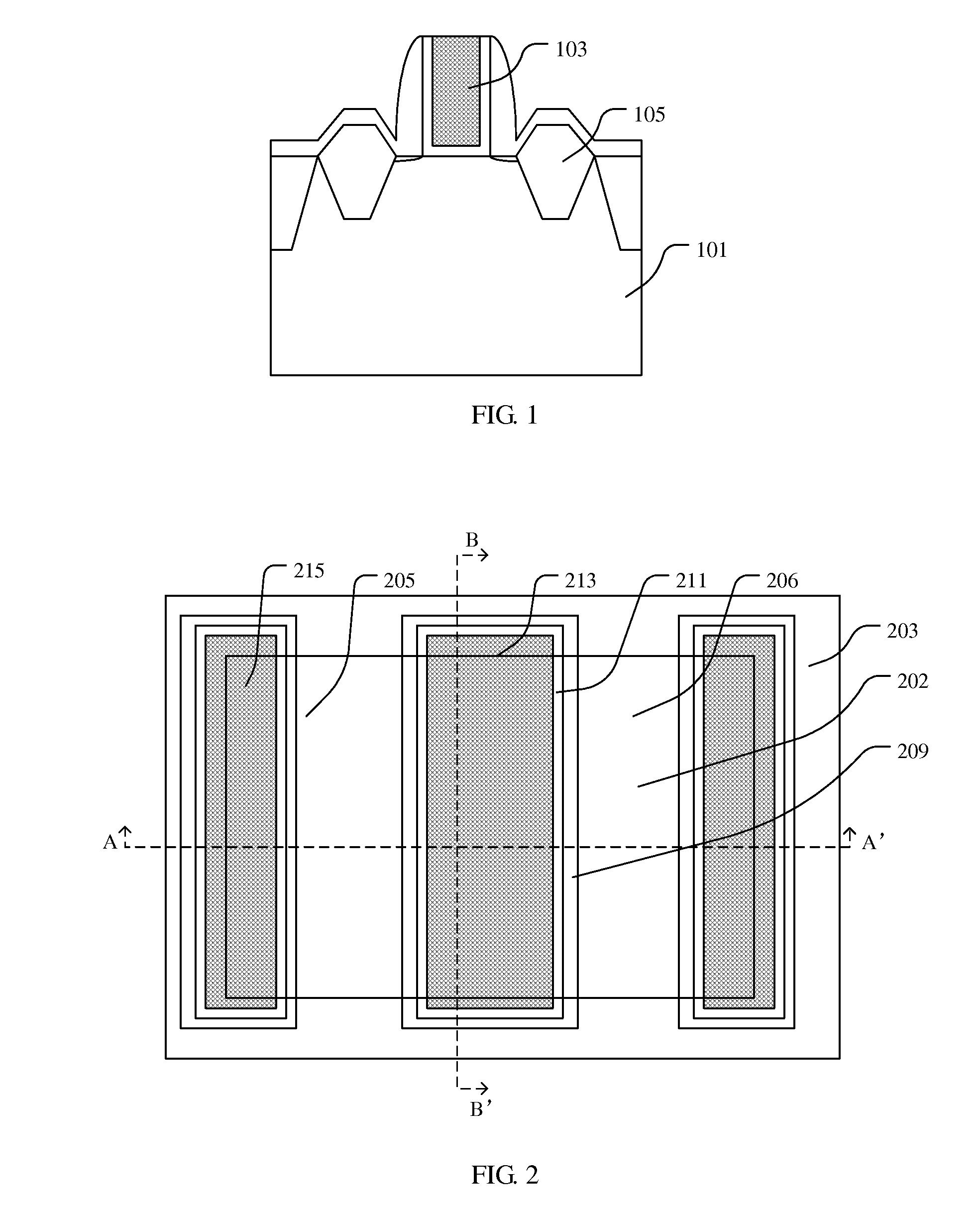
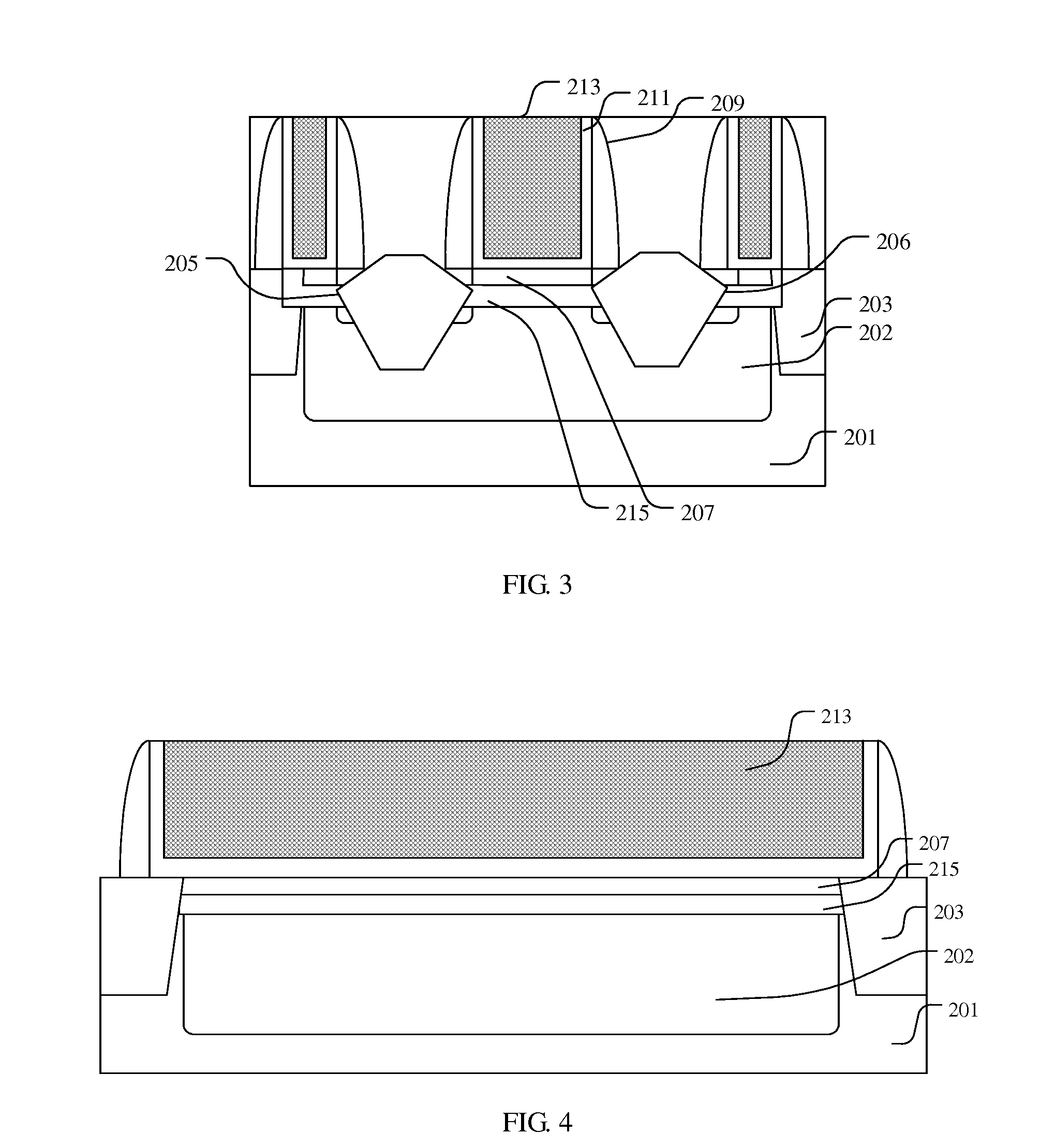
[0032]As described in the background, conventional MOS transistors have thick body regions, which are subject to the short channel effects and restricts further improvement of device performance. To solve this problem, the present invention provides a MOS transistor with ultra-thin body regions. The ultra-thin body transistor has a buried insulated region formed in the substrate. The buried insulated region isolates the body region under the gate from the substrate. Therefore, the thickness of the body region of the ultra-thin body transistor is greatly decreased, which greatly suppress the short channel effect.

[0033]In addition, for the ultra-thin body transistor provided in th...


PUM


Abstract

An ultra-thin body transistor and a method for manufacturing an ultra-thin body transistor are disclosed. The ultra-thin body transistor comprises: a semiconductor substrate; a gate structure on the semiconductor substrate; and a source region and a drain region in the semiconductor substrate and on either side of the gate structure; in which the gate structure comprises a gate dielectric layer, a gate embedded in the gate dielectric layer, and a spacer on both sides of the gate; the ultra-thin body transistor further comprises: a body region and a buried insulated region located sequentially under the gate structure and in a well region; two ends of the body region and the buried insulated region are connected with the source region and the drain region respectively; and the body region is isolated from other regions in the well region by the buried insulated region under the body region. The ultra-thin body transistor has a thinner body region, which decreases the short channel effect. In the method for manufacturing an ultra-thin body transistor together with the replacement-gate process, the forming of the buried insulated region is self-aligned with the gate, which reduces the parasitic resistance under the spacer.

Description

[0001]This application is a Section 371 National Stage Application of International Application No. PCT / CN2011 / 070686, filed on Jan. 27, 2011, which claims the benefit of No. 201010257023.2, filed on Aug. 18, 2010, the entire contents of which are incorporated herein by reference in their entirety.BACKGROUND OF THE INVENTION[0002]1. Field of the Invention[0003]The present invention relates to the semiconductor field, and particularly relates to an ultra-thin body transistor and manufacturing method thereof.[0004]2. Description of Prior Art[0005]With continuous development of semiconductor manufacturing technology, number of devices integrated in one chip has increased from several hundreds to today's several hundreds of millions. The performance and complexity of ICs have been advanced to an unimaginable level. To meet the requirements of complexity and circuit density, the minimum feature size is decreasing. Currently, a MOS transistor has a minimum line width of less than 45 nm.[0...

Claims


Application Information

Patent Timeline
IPC IPC(8): H01L29/772H01L21/336
CPCH01L21/28123H01L29/165H01L29/7834H01L29/66636H01L29/66545H01L29/66772H01L29/78654
Inventor LIANG, QINGQINGZHONG, HUICAIZHU, HUILONG
Owner INST OF MICROELECTRONICS CHINESE ACAD OF SCI
Why Eureka
Try Eureka