

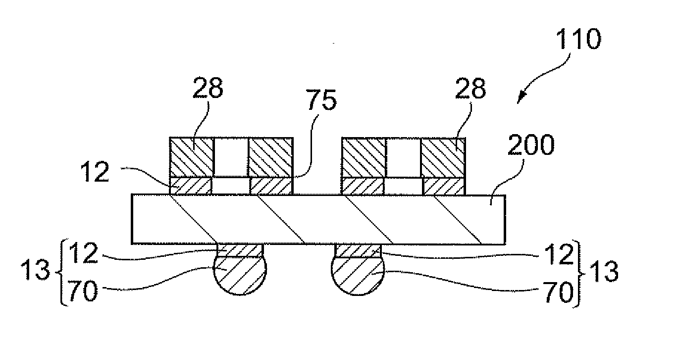
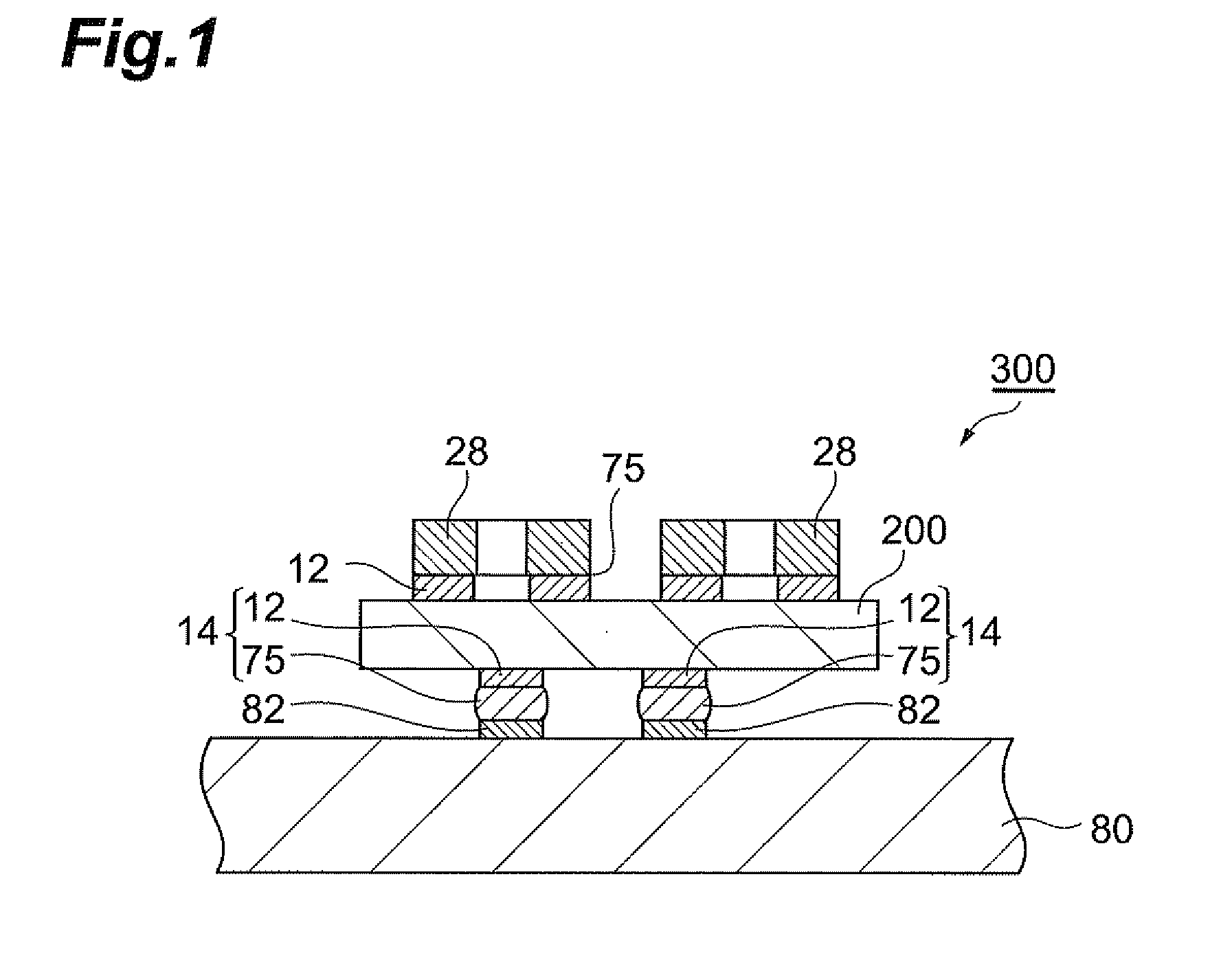
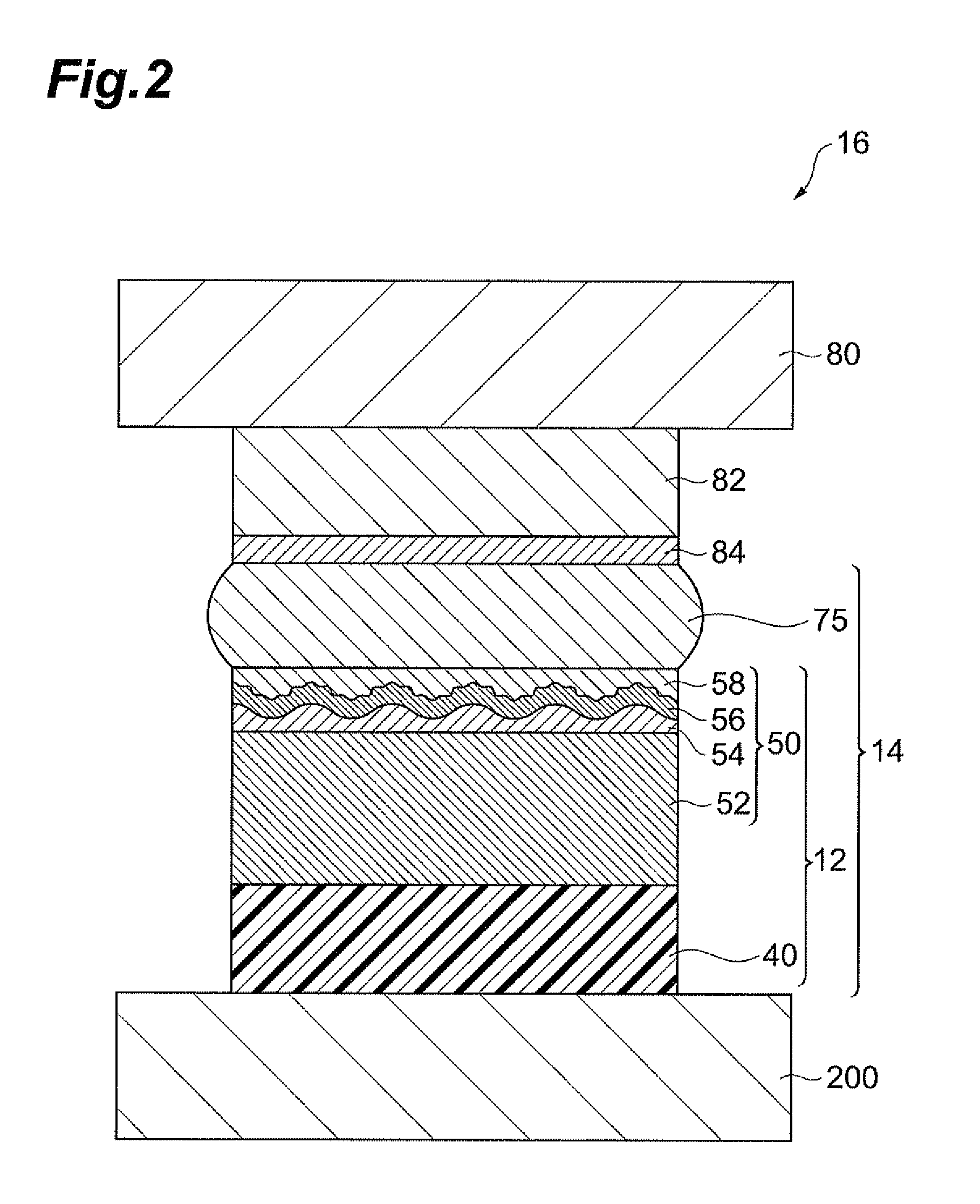
Terminal structure, printed wiring board, module substrate, and electronic device
a technology of printed wiring and terminal structure, applied in the direction of printed circuit manufacture, electrical apparatus construction details, capacitors, etc., can solve the problems of degrading soldering performance and wire bonding performance, and achieve excellent drop strength, suppress corrosion of the first and second layers, and improve drop strength
- Summary
- Abstract
- Description
- Claims
- Application Information
AI Technical Summary
Benefits of technology
Problems solved by technology
Method used
Image

Examples
example 1
[0092](Production of Package Substrate with Precursor Structures)
[0093]A high-heat-resistance substrate (product name: FR4, thickness: 3 mm, available from Hitachi Chemical Co., Ltd.) being a substrate for package was prepared. Through holes were formed in this substrate with an NC drill and then copper through-hole plating was carried out. Thereafter, an etching resist was formed in a predetermined shape and unnecessary copper wiring was removed by etching to form a daisy chain circuit pattern. Thereafter, in order to prevent precipitation of plated metal at unnecessary locations, the surface of the substrate was overcoated in part with a solder resist and then copper pads (φ0.6 mm) for connection of solder balls were formed.
[0094]A dummy silicon wafer 0.3 mm thick was bonded to one surface of the substrate with an adhesive. Thereafter, resin sealing was carried out to obtain the substrate with the total thickness of 1.1 mm. This substrate was subjected to the below-described steps...
PUM
| Property | Measurement | Unit |
|---|---|---|
| thickness | aaaaa | aaaaa |
| thickness | aaaaa | aaaaa |
| thickness | aaaaa | aaaaa |
Abstract
Description
Claims
Application Information