
Fluorene Derivative, Organic Compound, and Light-Emitting Element, Light-Emitting Device, and Electronic Device Using the Compound

a technology of organic compound and light-emitting element, which is applied in the direction of organic chemistry, thermoelectric devices, electric lighting sources, etc., can solve the problems of difficult to obtain a material having high triplet excitation energy and reduce emission efficiency, so as to improve the emission efficiency of light-emitting elements and reduce power consumption of light-emitting elements. , the effect of reducing the driving voltage of light-emitting elements

Inactive Publication Date: 2012-03-01
SEMICON ENERGY LAB CO LTD
View PDF6 Cites 9 Cited by
  • Summary
  • Abstract
  • Description
  • Claims
  • Application Information

AI Technical Summary

Benefits of technology

[0016]An object of one embodiment of the present invention is to reduce driving voltage of a light-emitting element. In addition, an object of one embodiment of the present invention is to improve emission efficiency of a light-emitting element.
[0017]In addition, an object of one embodiment of the present invention is to reduce power consumption of a light-emitting element, a light-emitting device, and an electronic device.
[0026]A fluorene derivative represented by General Formula (G1) has a bipolar property, and thus can be favorably used, as an organic semiconductor material, for a light-emitting element or an organic device such as an organic transistor.
[0028]In particular, since the organic semiconductor material represented by General Formula (G1) has high triplet excitation energy, it has more prominent effect when being used for a light-emitting element together with a phosphorescent compound.
[0036]Further, application of one embodiment of the present invention makes it possible to reduce driving voltage of a light-emitting element and improve emission efficiency of a light-emitting element.
[0037]Further, application of one embodiment of the present invention makes it possible to reduce power consumption of a light-emitting element, a light-emitting device, and an electronic device.

Problems solved by technology

When the light-emitting region locally exists, quenching due to triplet-triplet annihilation (T-T annihilation) is caused, which results in reduction in emission efficiency.
However, when a skeleton having an electron-transport property and a skeleton having a hole-transport property are directly bonded, decrease in band gap is caused, which makes it difficult to obtain a material having high triplet excitation energy.

Method used


Image

  • Fluorene Derivative, Organic Compound, and Light-Emitting Element, Light-Emitting Device, and Electronic Device Using the Compound
  • Fluorene Derivative, Organic Compound, and Light-Emitting Element, Light-Emitting Device, and Electronic Device Using the Compound
  • Fluorene Derivative, Organic Compound, and Light-Emitting Element, Light-Emitting Device, and Electronic Device Using the Compound

Examples


embodiment 1

[0056]In this embodiment, an organic semiconductor material below will be described as an example of an organic compound of the present invention.

[0057]The organic semiconductor material according to one embodiment of the present invention has a fluorene skeleton and a structure in which an electron-accepting unit and a hole-accepting unit are bonded through carbon at the 9-position of the fluorene skeleton.

[0058]Specifically, the organic semiconductor material of this embodiment is an organic semiconductor material represented by General Formula (G1).

[0059]In the formula, EA represents an electron-accepting unit and HA represents a hole-accepting unit. Note that in the case where a substance derived by replacing a fluorene group bonded to HA with hydrogen is represented by HAH and a substance derived by replacing a fluorene group bonded to EA with hydrogen is represented by EAH, among HAH, EAH, and fluorene, EAH has the highest electron affinity and HAH has the smallest ionization ...

embodiment 2

[0099]In this embodiment, a synthesis method of the organic semiconductor material represented by General Formula (G1) below, which is described in Embodiment 1, will be described. The organic semiconductor material described in Embodiment 1 is a material in which both an electron-transport unit and a hole-transport unit are bonded to carbon at the 9-position of fluorene. In other words, the organic semiconductor material is an asymmetric substance. However, two hydrogen bonded to a carbon at the 9-position of unsubstituted fluorene are completely the same in terms of energy and cannot be distinguished from each other, which makes it very difficult to synthesize the organic semiconductor material by coupling reaction of unsubstituted fluorene and the electron-transport unit and the hole-transport unit. The present inventors have conducted diligent studies in view of the above and have found out that the organic semiconductor material described in Embodiment 1 can be obtained by a sy...

embodiment 3

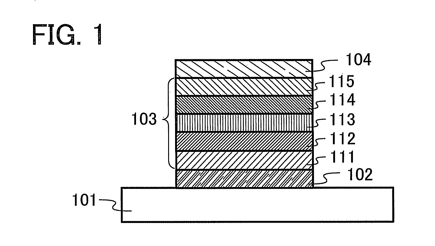
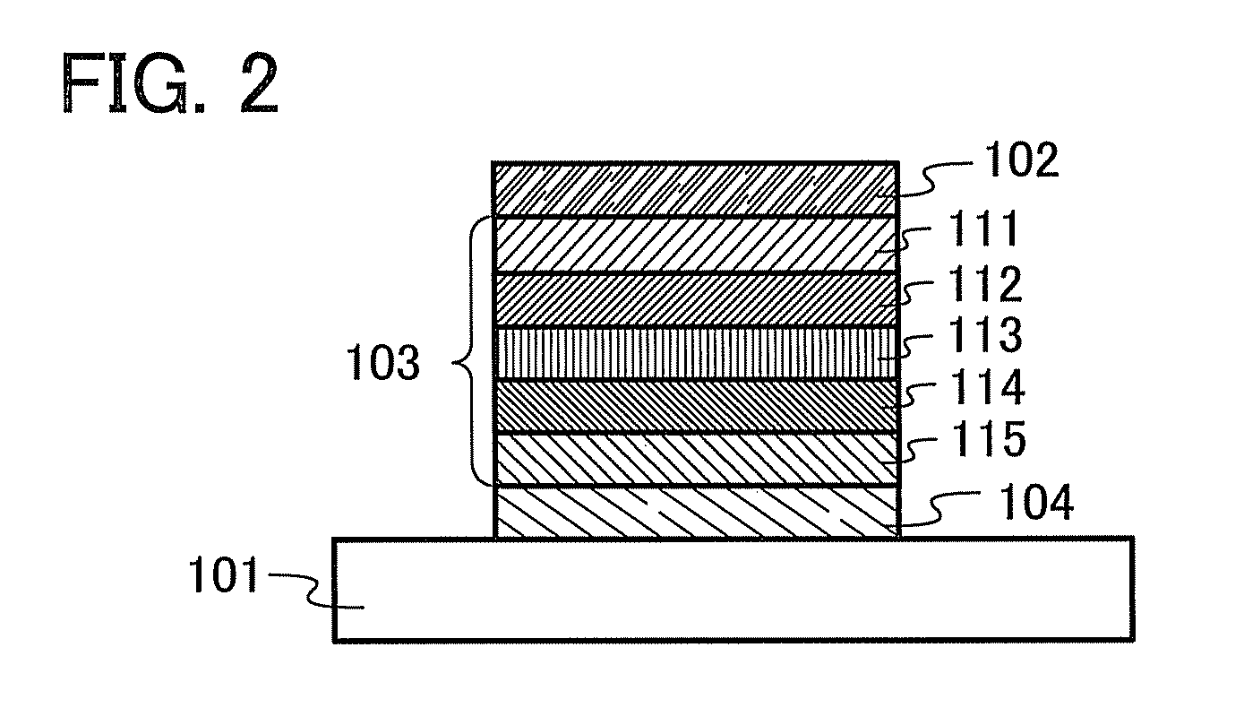
[0149]In this embodiment, one embodiment of a light-emitting element including the organic semiconductor material described in Embodiment 1 will be described with reference to FIG. 1 and FIG. 2.

[0150]The light-emitting element of the present invention includes a plurality of layers between a pair of electrodes. The plurality of layers is a combination of a layer containing a substance having a high carrier-injection property and a layer containing a substance having a high carrier-transport property which are stacked so that a light-emitting region is formed in a region away from the electrodes, that is, so that carriers recombine in a region away from the electrodes.

[0151]In this embodiment, the light-emitting element includes a first electrode 102, a second electrode 104, and an EL layer 103 provided between the first electrode 102 and the second electrode 104. Note that in this embodiment, description is made on the assumption that the first electrode 102 functions as an anode an...


PUM

PropertyMeasurementUnit
ionization potentialaaaaaaaaaa
internal quantum efficiencyaaaaaaaaaa

Abstract

To provide a novel organic compound having a bipolar property. To reduce power consumption of a light-emitting element, a light-emitting device, and an electronic device. The organic compound has a fluorene skeleton and a structure in which an electron-accepting unit and a hole-accepting unit are bonded through carbon at the 9-position of the fluorene skeleton. The organic compound has a bipolar property and a large band gap. The use of the organic compound makes it possible to reduce power consumption of a light-emitting element, a light-emitting device, and an electronic device.

Description

BACKGROUND OF THE INVENTION[0001]1. Field of the Invention[0002]The present invention relates to a fluorene derivative, an organic compound (an organic semiconductor material), and a light-emitting element, a light-emitting device, and an electronic device using the organic compound.[0003]2. Description of the Related Art[0004]An organic compound can take a variety of structures in comparison with an inorganic compound and can be used to synthesize a material having a variety of functions with appropriate molecular design. Owing to these advantages, electronics utilizing a functional organic material has been attracting attention in recent years.[0005]As examples of electronic devices using an organic compound as a functional material, there are solar cells, light-emitting elements, organic transistors, and the like. These are devices in which electric properties and optical properties of organic compounds are utilized. In particular, tremendous progress has been made in light-emitt...

Claims


Application Information

Patent Timeline
Patent Type & Authority Applications(United States)
IPC IPC(8): H05B37/02C07D235/18H01L51/54
CPCC07D235/18H01L51/0051H01L51/0059Y02E10/549H01L51/5016H01L51/504H01L51/0072H10K85/611H10K85/631H10K85/6572H10K50/11H10K2101/10H10K50/13
Inventor SEO, SATOSHIKAWAKAMI, SACHIKOOSAKA, HARUE
Owner SEMICON ENERGY LAB CO LTD
Learn More