Semiconductor device and light-emitting device

Active Publication Date: 2012-03-15
SEMICON ENERGY LAB CO LTD
View PDF13 Cites 13 Cited by
  • Summary
  • Abstract
  • Description
  • Claims
  • Application Information

AI Technical Summary

Benefits of technology

[0030]According to one embodiment of the present invention, a highly reliable semiconductor device including an oxide semic

Problems solved by technology

There is a problem in that a transistor having a channel formation region formed of an oxide semiconductor, which is of an enhancement (also referred to as normally-off) type, is changed into a depletion (also referred to as normally-on) type due to the use.
In particular, in a semiconductor device which includes an organic layer containing a light-emitting substance between a first electr

Method used


Image

  • Semiconductor device and light-emitting device
  • Semiconductor device and light-emitting device
  • Semiconductor device and light-emitting device

Examples


embodiment 1

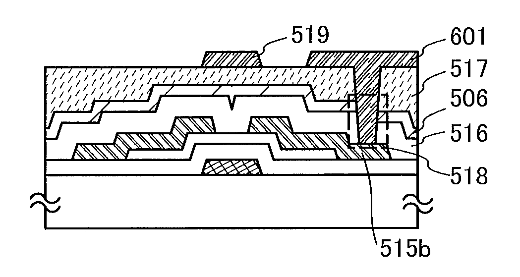
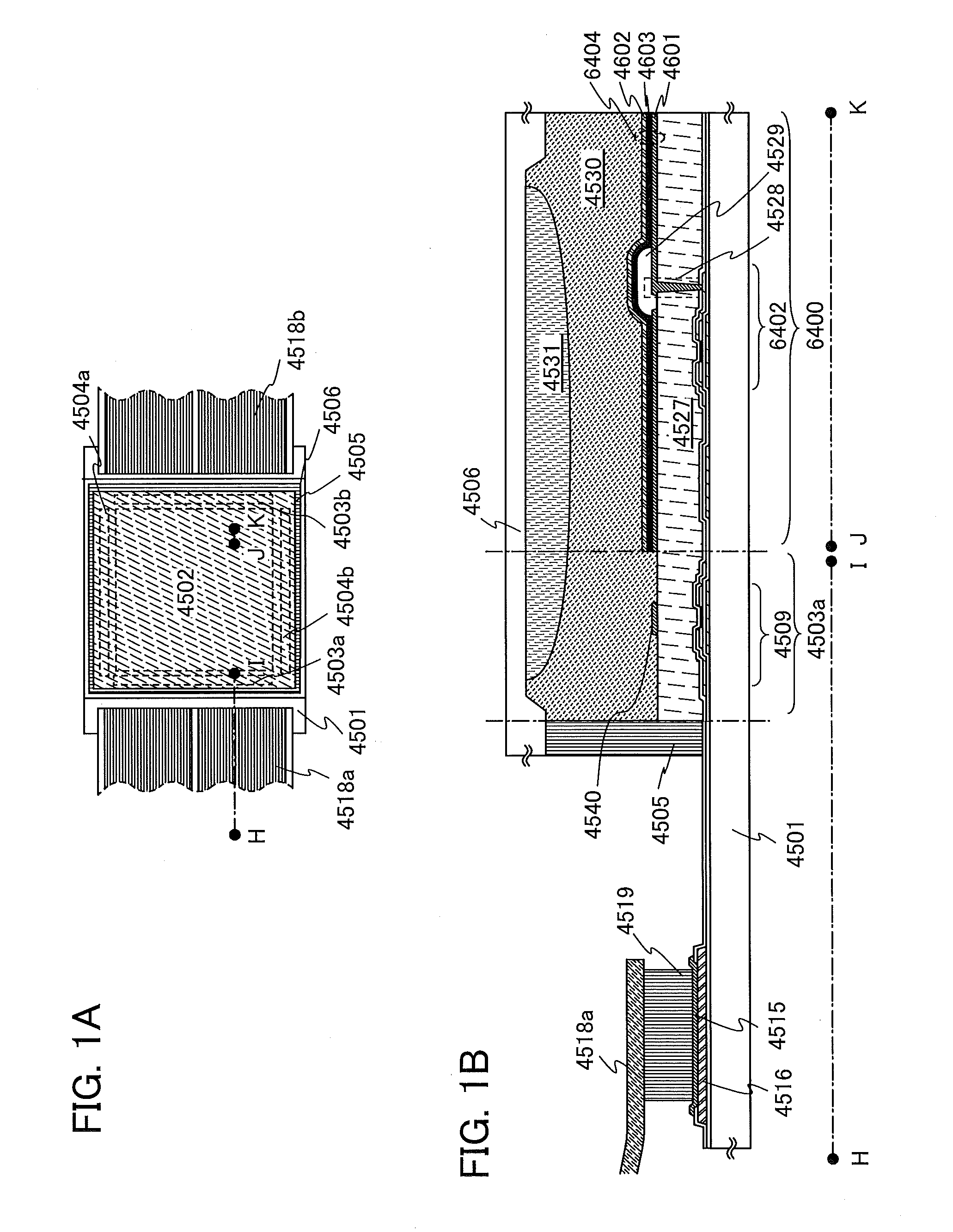
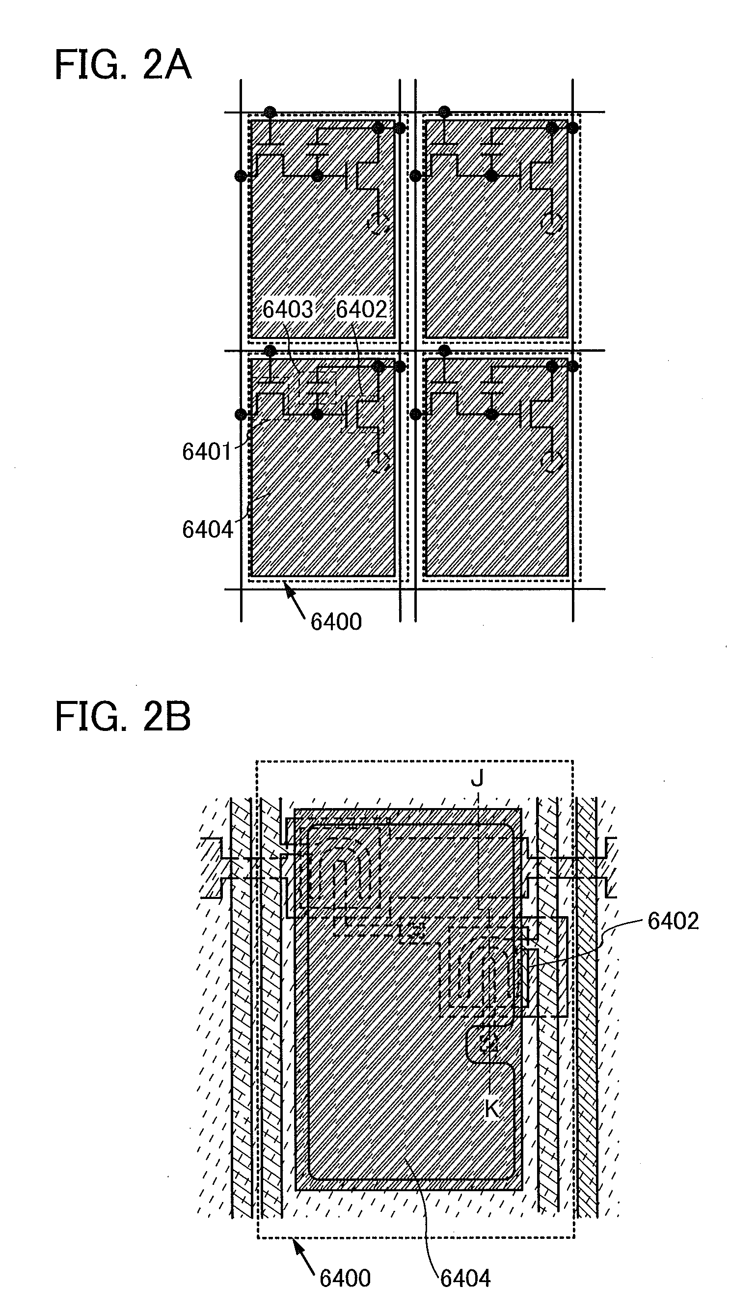
[0041]In this embodiment, a semiconductor device will be described. The semiconductor device includes an enhancement transistor having a channel formation region formed of an oxide semiconductor, and a light-emitting element including an organic layer containing a light-emitting substance between a first electrode connected to a source electrode or a drain electrode of the transistor through an opening provided in an interlayer insulating layer over the transistor and a second electrode overlapping with the first electrode. Further, the semiconductor device is provided with an adsorption layer of a hydrogen ion and / or a hydrogen molecule on the opposite surface side of the second electrode having one surface in contact with the organic layer. Specifically, a light-emitting display device (also referred to as a light-emitting display panel) will be described with reference to FIGS. 1A and 1B, FIGS. 2A and 2B, FIG. 3, FIG. 4, and FIG. 5.

[0042]FIG. 1A is a plan view of a light-emitting...

embodiment 2

[0086]In this embodiment, an enhancement transistor having a channel formation region formed of an oxide semiconductor will be described. An enhancement transistor having a channel formation region formed of an oxide semiconductor includes a gate electrode on one side of a gate insulating film, an oxide semiconductor layer on the other side of the gate insulating film, and a source electrode and a drain electrode which are in contact with the oxide semiconductor layer and whose end portions overlap with the gate electrode. In this embodiment, as an example of an enhancement transistor having a channel formation region formed of an oxide semiconductor, an example of a structure and a manufacturing method of an inverted staggered transistor including an oxide semiconductor will be described with reference to FIGS. 6A to 6E. Note that the transistor is not limited to an inverted staggered transistor, and the transistor may be a staggered transistor, a coplanar transistor, or an inverte...

embodiment 3

[0172]In this embodiment, an example of a structure and a manufacturing method of a light-emitting element that can be applied to the semiconductor devices described in Embodiment 1 will be described with reference to FIG. 8. Specifically, a light-emitting element including a first electrode serving as one of an anode and a cathode, which is electrically connected to a source electrode or a drain electrode of a transistor having a channel formation region formed of an oxide semiconductor, a second electrode serving as the other of the anode and the cathode, and an organic layer containing a light-emitting substance between the first electrode and the second electrode will be described.

[0173]Note that the structure of the light-emitting element described as an example in this embodiment can include the first electrode as an anode and the second electrode as a cathode. Alternatively, the first electrode can serve as a cathode and the second electrode can serve as an anode. Note that t...


PUM


Abstract

To provide a highly reliable semiconductor device including an oxide semiconductor. Further to provide a highly reliable light-emitting device including an oxide semiconductor. A second electrode sealed together with a semiconductor element including an oxide semiconductor hardly becomes inactive. A hydrogen ion and/or a hydrogen molecule produced by reaction of the active second electrode with moisture remaining in the semiconductor device and/or moisture entering from the outside of the device increase the carrier concentration in the oxide semiconductor, which causes a reduction in the reliability of the semiconductor device. An adsorption layer of a hydrogen ion and/or a hydrogen molecule may be provided on the other surface side of the second electrode having one surface in contact with the organic layer. Further, an opening which a hydrogen ion and/or a hydrogen molecule passes through may be provided for the second electrode.

Description

BACKGROUND OF THE INVENTION[0001]1. Field of the Invention[0002]The present invention relates to a semiconductor device and a light-emitting device each of which includes an oxide semiconductor.[0003]Note that in this specification, a semiconductor device refers to any device including a semiconductor element that functions by utilizing semiconductor properties, and semiconductor circuits, light-emitting devices, display devices, and electronic devices are all semiconductor devices.[0004]2. Description of the Related Art[0005]There are techniques by which a transistor is formed over a substrate having an insulating surface by using a semiconductor material such as amorphous silicon, polycrystalline silicon, or transferred single crystal silicon. While a transistor including amorphous silicon has low field-effect mobility, the transistor can be easily formed over a large glass substrate. On the other hand, while a transistor including polycrystalline silicon has relatively high field...

Claims


Application Information

Patent Timeline
IPC IPC(8): H01L29/786H01L33/00
CPCH01L27/1225H01L51/5259H01L29/78606H10K50/846H01L29/78642H01L29/7869H01L29/78696
Inventor HATANO, KAORU
Owner SEMICON ENERGY LAB CO LTD
Why Eureka
Try Eureka