Method of Contacting a Semiconductor Substrate

a technology of semiconductor substrates and contact points, which is applied in the direction of semiconductor devices, electrical equipment, photovoltaic energy generation, etc., can solve the problems of high temperature step, too expensive method, and loss of metal used,

Inactive Publication Date: 2012-04-05
UNIV STUTTGART
View PDF1 Cites 13 Cited by
  • Summary
  • Abstract
  • Description
  • Claims
  • Application Information

AI Technical Summary

Benefits of technology

[0025]This means that contact is made very cost-effectively and highly effectively without additional process steps. In a corresponding manner, the seed structure can be produced directly on the substrate surface through a passivation layer

Problems solved by technology

However, this method is too expensive for large-scale production, since a large number of process steps are required, and the majority of the metal used is lost by vapour deposition of the entire sample.
The disadvantages of this method are that a high-temperature step is required in order to make contact with the solar cell.
A further disadvantage is the aspect ratio of screen-printing lines, which limits the minimum line width to approximately 100 μm, with a line height of approximately 20 μm.
However, in this method, the contact must in general be subsequently treated at temperatures above 300° C. in order to achieve good resistance values, which means an additional process step, which furthermore re

Method used


Image

  • Method of Contacting a Semiconductor Substrate
  • Method of Contacting a Semiconductor Substrate
  • Method of Contacting a Semiconductor Substrate

Examples


Embodiment Construction

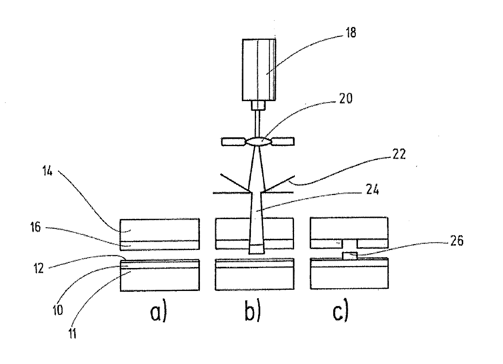
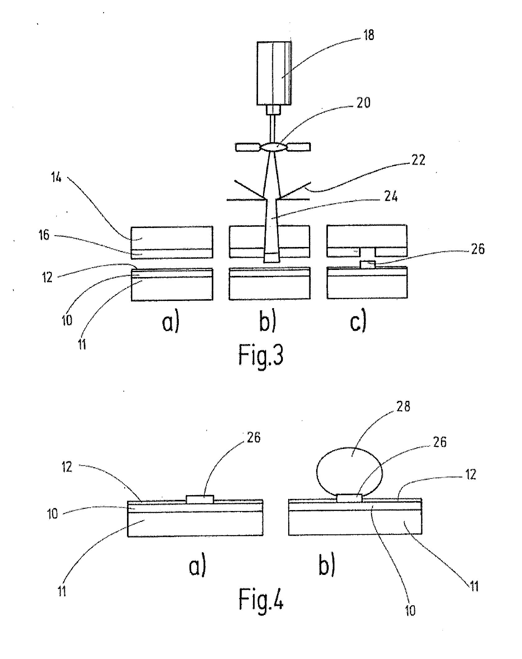
[0043]The principle of the LIFT process will be explained in more detail in the following text with reference to FIG. 3.

[0044]During the production of a solar cell, this solar cell must be provided with a metallic contact on the front face and on the rear face. By way of example, FIGS. 3a), b), c) show a p-type-doped base material (Si wafer or polycrystalline Si) which is annotated 11, on the front face of which a layer of n-type-doped material is located, which forms the emitter. This substrate layer 10 is provided with a cover layer 12, which is an antireflective layer, such as a silicon-nitride layer with a layer thickness of 50 to 100 nm.

[0045]A metallic seed structure 26 is now produced directly on the surface of the substrate layer 10, through the cover layer 12, by means of the LIFT process. For this purpose, a mount material 14 in the form of a thin glass layer or a thin film is arranged in the immediate vicinity in front of the substrate layer 10, and is provided with a thi...


PUM


Abstract

A method is disclosed for making contact with a semiconductor substrate, in particular for making contact with solar cells, in which a metallic seed structure is generated on the surface through a dielectric or passivating layer by means of an LIFT process, and the seed structure is then reinforced.

Description

CROSS REFERENCES TO RELATED APPLICATIONS[0001]This application is a continuation of International Patent Application PCT / EP2010 / 002364, filed on Apr. 17, 2010 designating the U.S., which International Patent Application has been published in German language and claims priority from German patent application 102009020774.0, filed on May 5, 2009. The entire contents of these applications is incorporated herein by reference.BACKGROUND OF THE INVENTION[0002]The invention relates to a method for contacting a semiconductor substrate, in particular for contacting solar cells.[0003]On a small scale, contact can be made particularly well with solar cells by vapour deposition of lithographically prestructured samples. However, this method is too expensive for large-scale production, since a large number of process steps are required, and the majority of the metal used is lost by vapour deposition of the entire sample.[0004]For this reason, the screen-printing process is widely used in industr...

Claims


Application Information

Patent Timeline
IPC IPC(8): H01L31/02H01L31/18
CPCH01L24/11H01L2924/0002H01L2224/13099H01L2924/01013H01L2924/0102H01L2924/01022H01L2924/01029H01L2924/01047H01L2924/0106H01L2924/01082H01L2924/01005H01L2924/01006H01L2924/01033H01L2224/03334H01L24/03H01L24/05H01L24/13H01L2224/03003H01L2224/031H01L2224/05655H01L2224/13023H01L2224/05568H01L2224/13006H01L31/022425H01L2924/00014Y02E10/50H01L2224/0401H01L2924/0001H01L2924/00013H01L2224/13599H01L2224/05599H01L2224/05099H01L2224/29099H01L2224/29599H01L2224/05552H01L2224/03505H01L31/0224H01L31/04H01L31/18
Inventor GRABITZ, PETERKOEHLER, JUERGENROEDER, TOBIASWERNER, JUERGEN H.
Owner UNIV STUTTGART
Why Eureka
Try Eureka