Printed circuit board

a printed circuit board and circuit board technology, applied in logic circuit coupling/interface arrangement, duplex signal operation, baseband system details, etc., can solve the problem of difficult to discriminate a digital signal symbol, the operation margin of the circuit deteriorates, and the previously transmitted signal becomes a noise for the currently transmitted signal

Inactive Publication Date: 2012-04-19
CANON KK
View PDF3 Cites 2 Cited by
  • Summary
  • Abstract
  • Description
  • Claims
  • Application Information

AI Technical Summary

Benefits of technology

[0021]In these circumstances, an object of the present invention is to provide a printed circuit board in which a timing jitter caused by intersymbol interference reduces using a passive component even in a case where output impedance of a transmission circuit and impedance of a transmission line are not matching with each other.

Problems solved by technology

In recent years, it becomes difficult to discriminate a symbol of a digital signal due to intersymbol interference in a transmission line on a printed circuit board as transmission speed of the digital signal in electronic equipment becomes higher, whereby an operation margin of the circuit deteriorates.
In a case where signal transmission speed is high, a next digital signal is transmitted before the waveform of a previously transmitted digital signal converges, whereby the previously transmitted signal becomes a noise for the currently transmitted signal.
In any case, it is said that, when the signal transmission speed exceeds 1 Gbps, the intersymbol interference becomes conspicuous and thus affects a circuit operation.
When the signal transmission speed exceeds 1 Gbps, a high-frequency component of a signal attenuates due to a skin effect and a dielectric loss on the transmission line, and thus the waveform of the signal becomes dull.
That is, the waveform of the signal output from a transmission terminal is dull at a receiving end due to attenuation of the high-frequency component of the signal on the transmission line.
When the widths 801 and 802 increase, it becomes impossible to obtain the signal amplitude sufficient for the circuit operation, whereby a voltage margin of the circuit deteriorates.
Further, when a starting voltage of a symbol change is different, a time margin of the circuit deteriorates.
However, when the circuit having the amplitude correction function is built into the semiconductor device, the area of the semiconductor device resultingly increases, and also power consumption resultingly increases.
However, in U.S. Patent Application Publication 2006 / 0197679, a problem that the timing jitter could not be reduced when the output impedance of the transmission circuit and the impedance of the transmission line were not matching with each other turned out.

Method used


Image

  • Printed circuit board
  • Printed circuit board
  • Printed circuit board

Examples


first embodiment

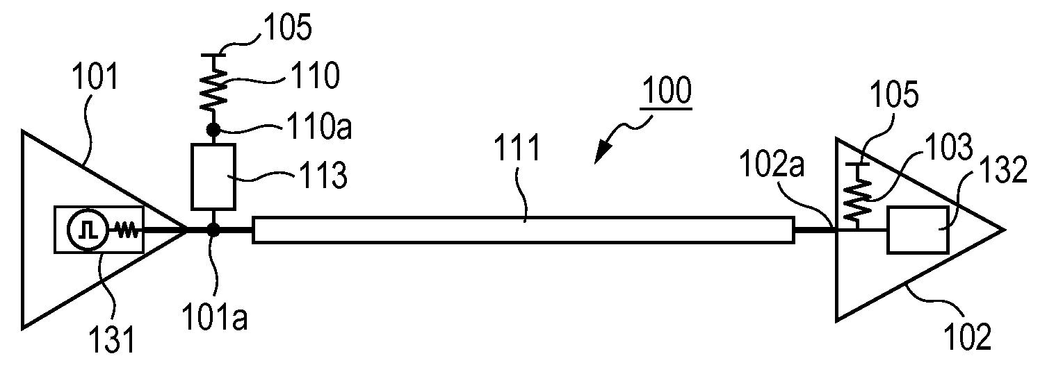
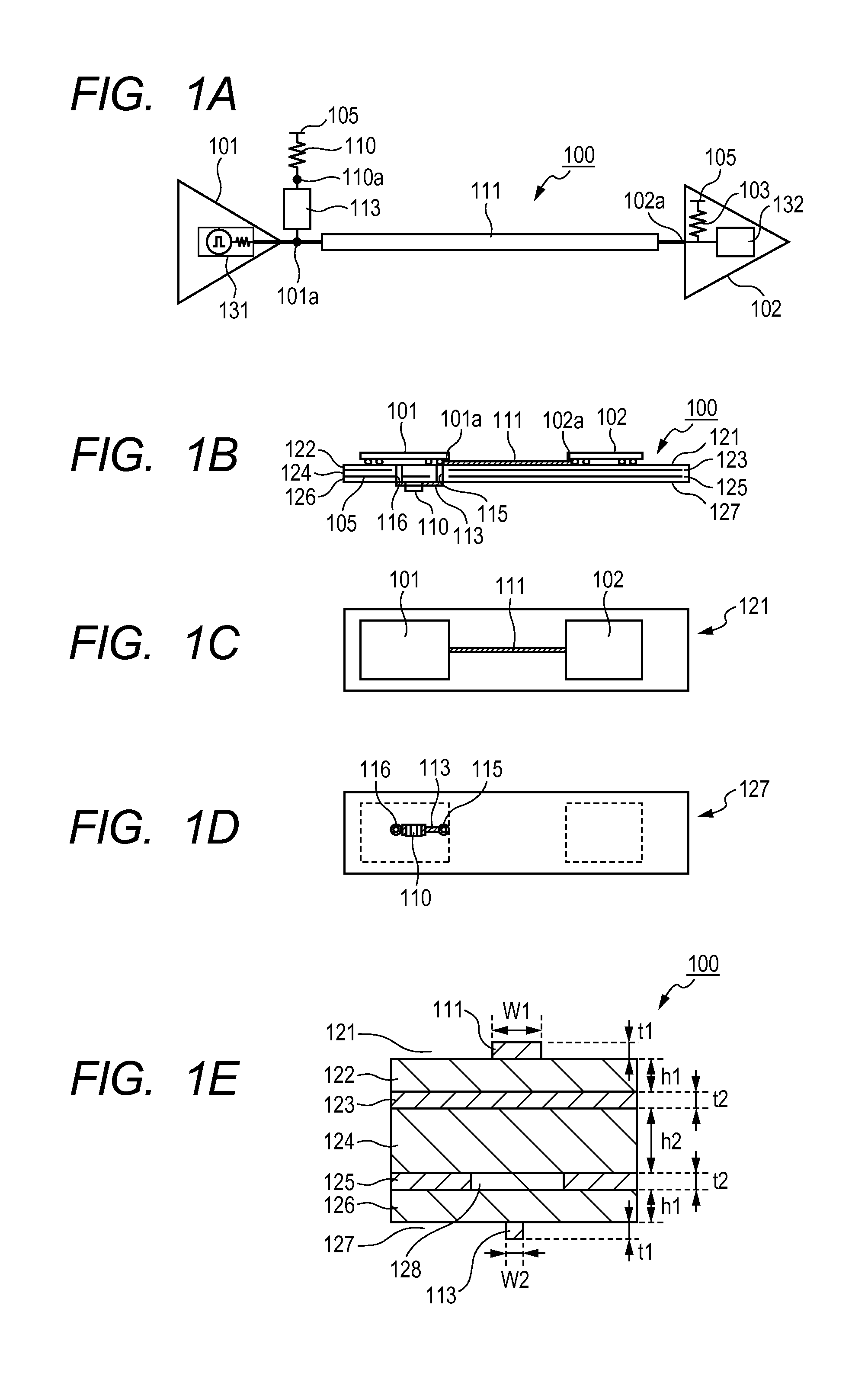
[0034]FIGS. 1A, 1B, 1C, 1D and 1E are explanatory diagrams illustrating a schematic constitution of a printed circuit board according to a first embodiment of the present invention. FIG. 1A illustrates an equivalent circuit of the printed circuit board. FIG. 1B is a cross-sectional view of the printed circuit board illustrated along the direction parallel with a main transmission line, and FIGS. 1C and 1D are plan views of signal wiring layers respectively formed on upper and rear surfaces of the printed circuit board. FIG. 1E is a cross-sectional view illustrated along the direction orthogonal to the main transmission line of the printed circuit board.

[0035]As indicated in FIG. 1A, a printed circuit board 100 has a transmission device 101, which has a built-in transmission circuit 131 for transmitting a signal, and a receiving device 102, which has a built-in receiving circuit 132 for receiving a signal. A signal output by the transmission circuit 131 is a digital signal, which is ...

example 1

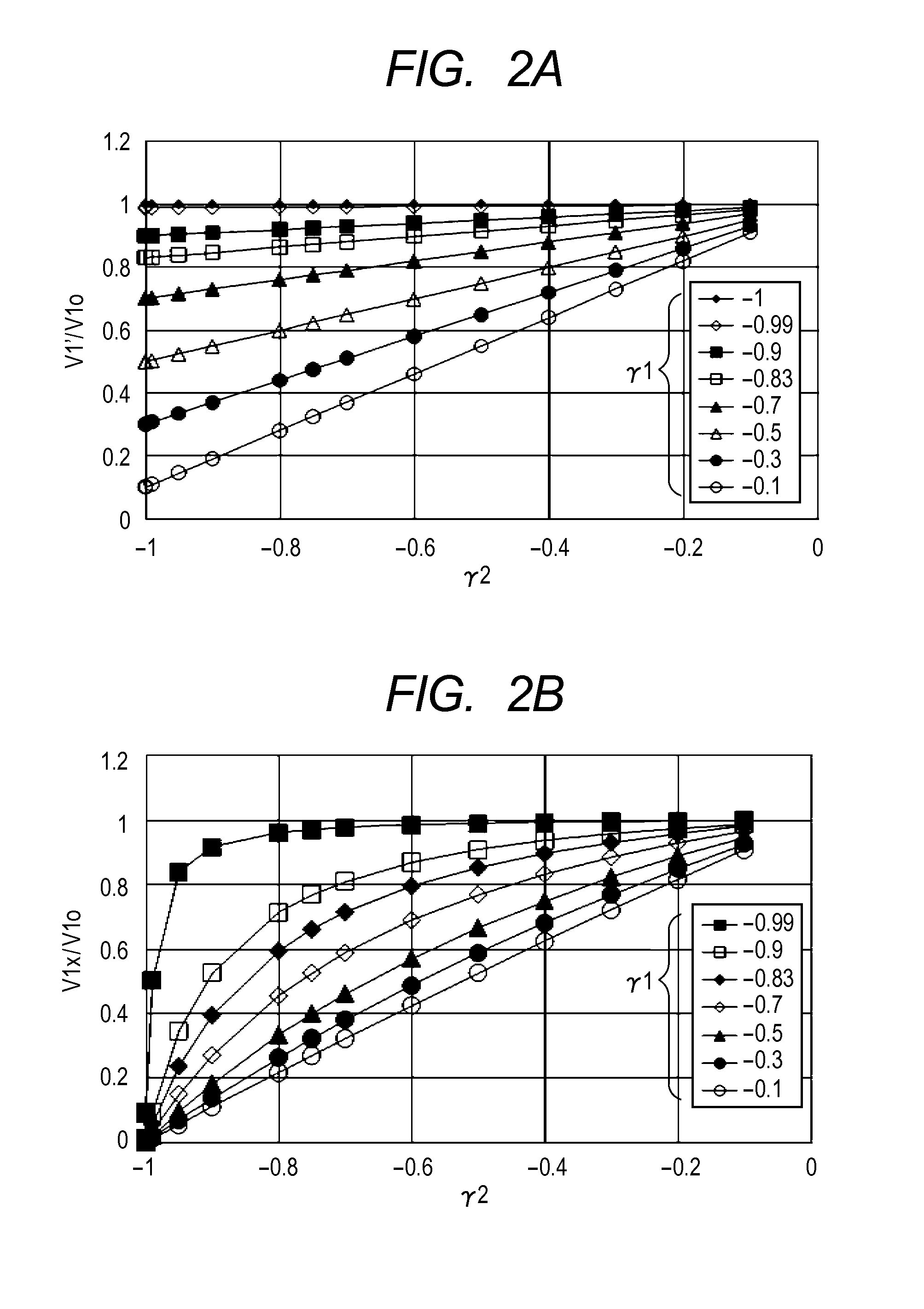
[0078]An effect of the first embodiment will be indicated by the computer simulation. Parameters of the respective portions used in the simulation will be indicated in the following description. First, parameters of the transmission device 101 will be indicated. An operation frequency was set as 2 [Gbps] (minimum pulse width Tmin was set as 500 [psec]), an amplitude range of the output saturation voltage was set as 0.9±0.9 [V] and the output impedance value R101 of the transmission circuit 131 was set as 20[Ω]. In addition, an output signal rising time (falling time) Tr was set as 100 [psec].

[0079]Next, parameters of the transmission line 111 will be indicated. The length of the transmission line 111 was set as 700 [mm] and the impedance value Z111 of the transmission line 111 was set as 50[Ω]. Next, parameters of the receiving circuit 132 will be indicated. The input threshold voltage was set as 0.9±0.25 [V], the resistance value R103 of the terminating resistor 103 was set as 50[Ω...

second embodiment

[0097]Next, a printed circuit board according to the second embodiment of the present invention will be described in detail. FIGS. 5A, 5B, 5C, 5D and 5E are explanatory diagrams illustrating a schematic constitution of a printed circuit board according to the second embodiment of the present invention. FIG. 5A illustrates an equivalent circuit of the printed circuit board. FIG. 5B is a cross-sectional view illustrated along the direction parallel with a main transmission line of the printed circuit board and FIGS. 5C and 5D are plan views of signal wiring layers of the printed circuit board. FIG. 5E is a cross-sectional view illustrated along the direction orthogonal to the main transmission line of the printed circuit board.

[0098]As indicated in FIG. 5A, a printed circuit board 200 has a differential transmission device 201, which has a built-in transmission circuit 231 for transmitting two differential signals and a differential receiving device 202, which has a built-in receiving...


PUM


Abstract

One end of a sub transmission line of which an impedance value is equal to or higher than a parallel impedance value of an output impedance value of a transmission circuit and an impedance value of a transmission line is connected to a connection point between the transmission circuit and the transmission line, and a correction resistor of which resistance is lower than an impedance value of the sub transmission line is connected to the other end of the sub transmission line. A length of the sub transmission line is set to satisfy a condition of 0.5×Tr (signal rise time)≦Td (signal propagation time of sub transmission line)≦0.5×Tmin (signal minimum pulse width), thereby achieving a de-emphasis function by a passive component, correcting a high-frequency component of a signal attenuated on the transmission line, and thus reducing timing jitters caused by intersymbol interference.

Description

BACKGROUND OF THE INVENTION[0001]1. Field of the Invention[0002]The present invention relates to a printed circuit board by which signal noises, particularly intersymbol interference, can be reduced.[0003]2. Description of the Related Art[0004]In recent years, it becomes difficult to discriminate a symbol of a digital signal due to intersymbol interference in a transmission line on a printed circuit board as transmission speed of the digital signal in electronic equipment becomes higher, whereby an operation margin of the circuit deteriorates. Here, it should be note that the intersymbol interference is the interference which occurs between temporally adjacent digital symbols. In a case where signal transmission speed is high, a next digital signal is transmitted before the waveform of a previously transmitted digital signal converges, whereby the previously transmitted signal becomes a noise for the currently transmitted signal. In any case, it is said that, when the signal transmi...

Claims


Application Information

Patent Timeline
Patent Type & Authority Applications(United States)
IPC IPC(8): H04B1/38H04L25/02
CPCH05K1/025H05K1/0245H01P1/26H03K19/0175H05K1/02
Inventor MATSUMOTO, SHOJI
Owner CANON KK
Why Eureka
Try Eureka