Flat panel display, intermediate manufactured product and method of manufacturing same

a technology of manufactured products and flat panels, applied in the manufacture of electric discharge tubes/lamps, discharge tubes luminescnet screens, instruments, etc., can solve the problems of increasing the manufacturing time and the cost of forming the color conversion layer b>540/b>, and achieves shortening the manufacturing time, low cost, and fineness. , the effect of increasing the fineness

Inactive Publication Date: 2012-04-26
FUJI ELECTRIC CO LTD
View PDF3 Cites 11 Cited by
  • Summary
  • Abstract
  • Description
  • Claims
  • Application Information

AI Technical Summary

Benefits of technology

[0014]Hence an object of this invention is, when using an application method to form a color conversion layer or similar on a structure having a bank, to either raise the fineness while using a conventional material and apparatus, or to perform application in greater quantities at a specific fineness to shorten the manufacturing time, so that a high-fineness, low-cost organic EL display or other flat panel display is provided.

Problems solved by technology

As a result, manufacturing time increases, and the cost of forming the color conversion layer 540 rises.

Method used


Image

  • Flat panel display, intermediate manufactured product and method of manufacturing same
  • Flat panel display, intermediate manufactured product and method of manufacturing same
  • Flat panel display, intermediate manufactured product and method of manufacturing same

Examples


example 1

Practical Example 1

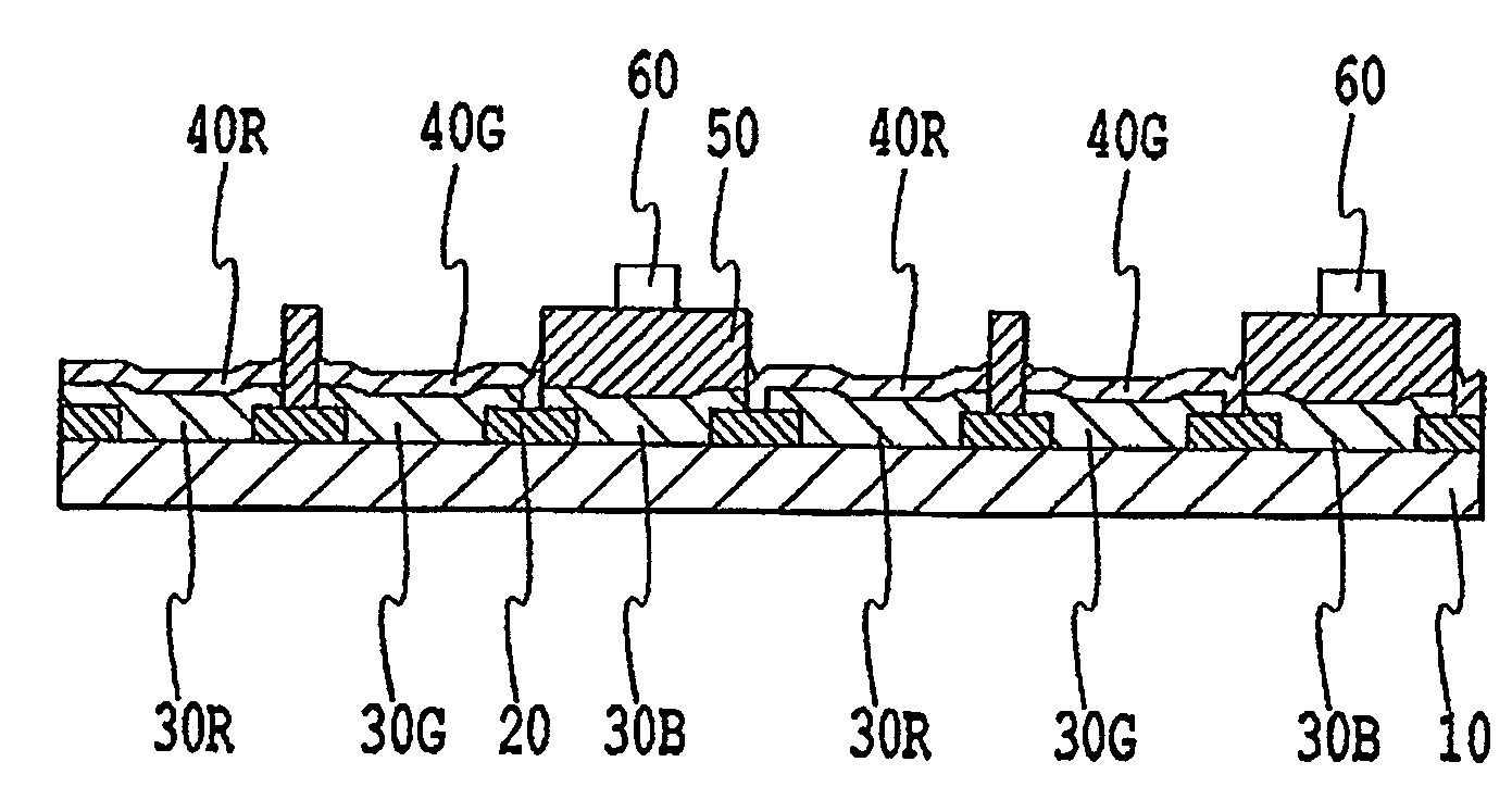
[0153]This practical example relates to an organic EL display having the structure of FIG. 7 and a nominal dimension of approximately 3 inches. Pixels in the organic EL display of this practical example are arranged at a pitch of 150 μm×150 μm. Each pixel is formed from red, green, and blue subpixels, arranged with a pitch of 50 μm×150 μm.

[0154]On a substrate 110 comprising alkali-free glass (AN-100, manufactured by Asahi Glass Co., Ltd.) 200×200 mm×thickness 0.7 mm, a plurality of switching elements 120 for a screen, formed from TFTs and similar, and wiring therefore, were formed. Next, a planarization layer 130 of film thickness 3 μm and an SiO2 passivation layer of film thickness 300 nm were formed so as to cover the switching elements 120, and contact holes for connection to the switching elements 120 were formed in the planarization layer 130 and passivation layer. Next, an RF magnetron sputtering apparatus was used to form an IZO film with a film thickness o...

example 2

Practical Example 2

[0167]This practical example relates to an organic EL display having the structure of FIG. 8. First, the procedures of Practical Example 1 was repeated to form an organic EL emission substrate 2.

[0168]Next, a procedure similar to that of Practical Example 1 was used to form a black matrix 20, red color filter 30R and green color filter 30G on a transparent substrate 10, comprising 200×200 nm×0.7 nm thick alkali-free glass (Eagle 2000, manufactured by Corning Inc.). In this practical example, formation of a blue color filter 30B was omitted.

[0169]Next, Color Mosaic (a registered trademark) CB-7001 was diluted, and the dye concentration was reduced to prepare a blue material. Then, except for using this blue material in place of the photosensitive resin (CR-600, manufactured by Hitachi Chemical Co., Ltd.), the procedure of Practical Example 1 for formation of the bank 50 was employed to form a blue bank 50B. At this time, the applied film thickness of the blue mater...

example 3

Practical Example 3

[0172]This practical example relates to an organic EL display with the structure of FIG. 9.

[0173]First, procedures similar to those of Practical Example 1 were used to form, on a transparent substrate 110 comprising 200×200 nm×0.7 nm thick alkali-free glass (AN-100, manufactured by Asahi Glass Co., Ltd.), constituent layers from the switching elements 120 to the transparent electrode 170.

[0174]Next, the layered member with the transparent electrode 170 formed was moved into a CVD apparatus without breaking the vacuum. A CVD method was used to form twice in alternation, on the entire substrate face, SiN of film thickness 0.5 μm and SiON of film thickness 0.5 μm, to form a barrier layer 180 of film thickness 2 μm.

[0175]Next, an ultraviolet-hardening resin, such as is used in microlens formation and similar, was diluted with a solvent, and a bank formation application liquid was prepared. Then, the bank formation application liquid was applied onto the barrier layer ...


PUM


Abstract

The present invention aims at providing a structure, manufacturing method, and an intermediate manufactured product enabling the low-cost manufacture of a flat panel display with high fineness. In a flat panel display of the invention, by decentering the opening portions formed by a bank in red and green subpixels to the blue subpixel side, color conversion layers with higher fineness can be formed even when using conventional apparatuses and materials. Moreover, decentering of the opening portions of the bank enables reductions in manufacturing time and manufacturing cost.

Description

TECHNICAL FIELD[0001]The present invention relates principally to a flat panel display, an intermediate manufactured product thereof, and a method of manufacturing same. More specifically, the present invention relates to an organic EL display, an intermediate manufactured product thereof, and a method of manufacturing same.BACKGROUND ART[0002]In a representative configuration of the panel unit of an organic EL display with a top-emission structure, an organic EL emission substrate (TFT substrate) and a color filter substrate are bonded together.[0003]An organic EL substrate known in the prior art includes a supporting substrate; a plurality of switching elements (TFTs or similar), existing at positions forming a plurality of subpixels; a planarization resin layer, covering the switching elements, and planarizing the upper face thereof; a reflective electrode, comprising a plurality of partial electrodes, connected to the switching elements via contact holes provided in the planariz...

Claims


Application Information

Patent Timeline
Patent Type & Authority Applications(United States)
IPC IPC(8): H05B33/14H01J9/00G02B5/22H01J5/16
CPCG02B5/201H01L27/3246H01L27/322H01L27/3211H10K59/35H10K59/38H10K59/122H10K50/865
Inventor NAKAMURA, HIDEYO
Owner FUJI ELECTRIC CO LTD
Why Eureka
Try Eureka