Workpiece dividing method

a workpiece and dividing technology, applied in the direction of basic electric elements, semiconductor/solid-state device manufacturing, electric apparatus, etc., can solve the problems of film being difficult to break, reducing etc., and achieve the effect of improving the die strength of each device obtained by dividing the workpi

Active Publication Date: 2012-04-26
DISCO CORP
View PDF25 Cites 13 Cited by
  • Summary
  • Abstract
  • Description
  • Claims
  • Application Information

AI Technical Summary

Benefits of technology

[0011]According to the present invention, even when the film such as a metal film is present on the streets of the workpiece, the w...

Problems solved by technology

In the above related-art method of dividing a workpiece by applying a laser beam to the workpiece to form the modified layers in the workpiece, there is a problem such that when a film such as a metal film is present on the streets ...

Method used


Image

  • Workpiece dividing method
  • Workpiece dividing method
  • Workpiece dividing method

Examples


Embodiment Construction

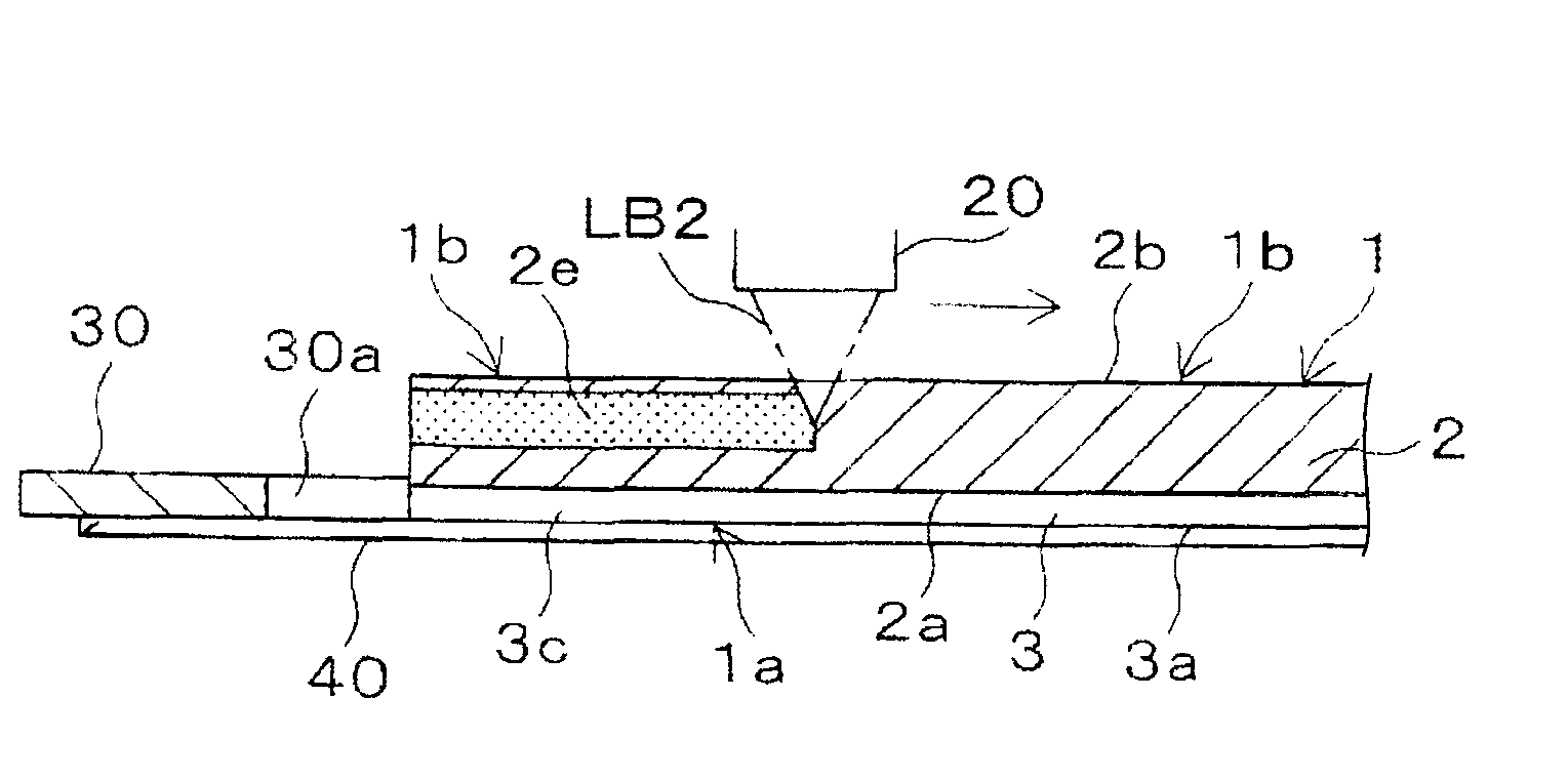
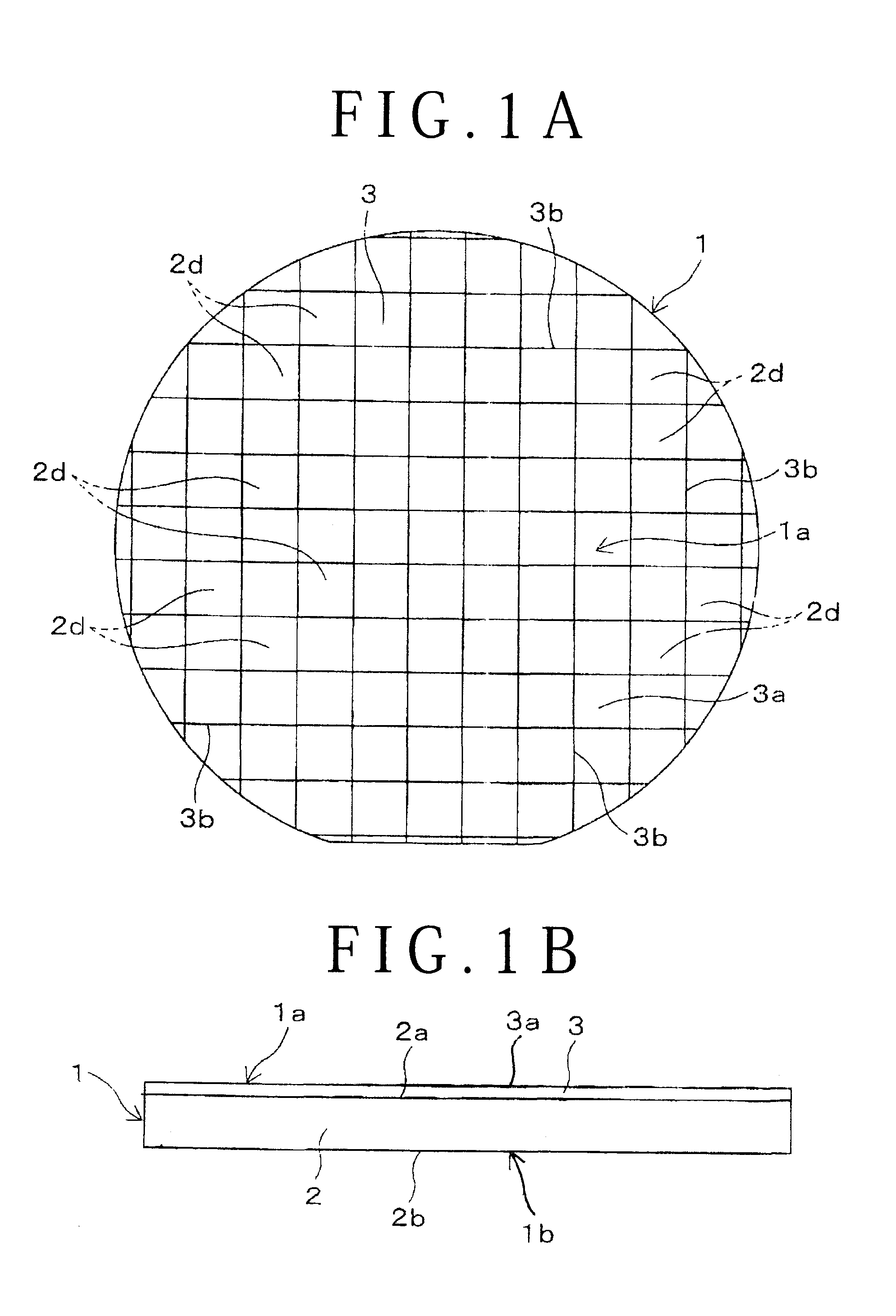
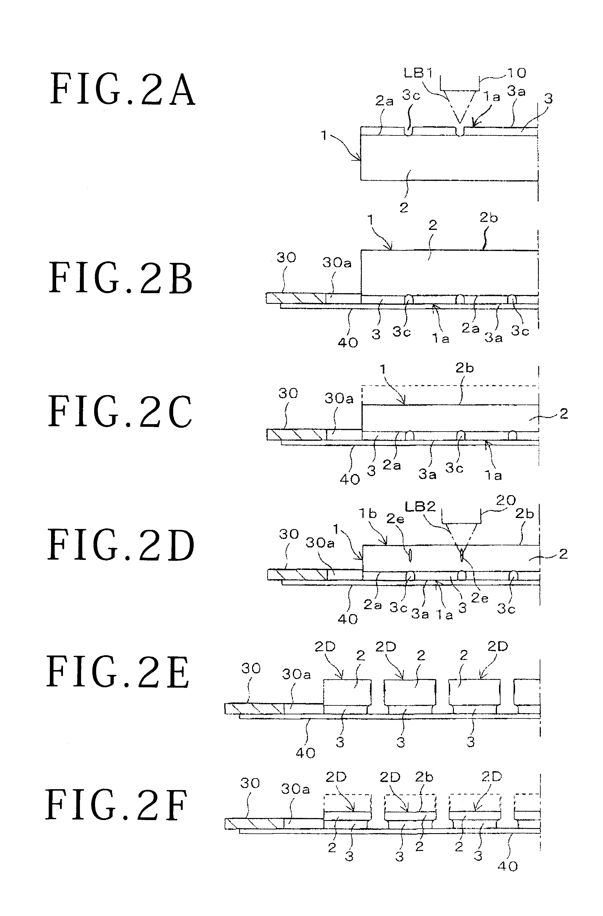
[0019]A preferred embodiment of the present invention will now be described in detail with reference to the drawings. Reference numeral 1 in FIG. 1A generally denotes a disk-shaped workpiece to be divided by a dividing method according to a preferred embodiment of the present invention. As shown in FIG. 1B, the workpiece 1 is composed of a disk-shaped substrate 2 such as a semiconductor wafer and a film 3 formed on the front side 2a of the substrate 2. The substrate 2 has a thickness of about 600 to 700 μm, for example, and the film 3 has a thickness of about 20 to 30 μm, for example.

[0020]As shown in FIG. 1A, a plurality of crossing streets 3b are formed on the front side 3a of the film 3 to thereby partition the substrate 2 into a plurality of rectangular device regions 2d. A device (not shown) such as IC, LSI, liquid crystal driver, and flash memory is formed on the front side of each device region 2d. The film 3 is formed from a metal film, fluorosilicate glass film, etc. as men...


PUM


Abstract

A workpiece has a substrate and a film formed on the front side of the substrate. A first laser beam applied to the film from the front side of the workpiece along streets formed on the film, thereby forming a plurality of laser processed grooves along the streets. An adhesive tape is attached to the front side of the workpiece. Thereafter, a second laser beam is applied to the substrate from the back side of the workpiece along the streets, with the focal point of the second laser beam set inside the substrate, forming a plurality of modified layers along the streets. Thereafter, the adhesive tape is expanded to divide the substrate along the streets, thereby obtaining a plurality of individual devices. The back side of the substrate of each device is then ground to remove the modified layers and reduce the thickness of each device to a predetermined thickness.

Description

BACKGROUND OF THE INVENTION[0001]1. Field of the Invention[0002]The present invention relates to a workpiece dividing method suitably applicable in the case of dividing a workpiece such as a semiconductor wafer to obtain a plurality of devices.[0003]2. Description of the Related Art[0004]In a semiconductor device fabrication process, a plurality of crossing division lines called streets are formed on the front side of a workpiece such as a disk-shaped semiconductor wafer to thereby partition a plurality of rectangular device regions where a plurality of devices such as ICs, LSIs, liquid crystal drivers, and flash memories are respectively formed on the front side. After grinding the back side of the workpiece and next performing necessary processing such as polishing, the workpiece is cut along the streets to divide the device regions, thus obtaining the individual devices.[0005]In general, the division of the workpiece is performed by using a cutting apparatus called a dicing saw h...

Claims


Application Information

Patent Timeline
IPC IPC(8): H01L21/78
CPCH01L21/78
Inventor NAKAMURA, MASARU
Owner DISCO CORP
Why Eureka
Try Eureka