Semiconductor structure and method for manufacturing the same

a semiconductor and semiconductor technology, applied in the field of semiconductor structure and manufacturing, can solve the problems of increasing the area occupied by the device, deteriorating the performance of the device, and reducing the integration level of the soi mosfet, so as to reduce the manufacturing cost, improve the integration level, and improve the effect of the manufacturing process

Active Publication Date: 2012-05-03
INST OF MICROELECTRONICS CHINESE ACAD OF SCI
View PDF2 Cites 194 Cited by
  • Summary
  • Abstract
  • Description
  • Claims
  • Application Information

AI Technical Summary

Benefits of technology

[0042]The semiconductor structure adjusts a threshold voltage with a common contact, which leads to a simple manufacturing process, an increased integration level and a lowered manufacture cost. Moreover, the asymmetric design of the back-gate structure further increases the threshold voltage and improves the performance of the device.

Problems solved by technology

However, reduction of gate pitch may lead to short channel effects, which deteriorate performance of the device.
Thus, the fully depleted SOI MOSFET having an ultra-thin body and a double gate attracts a great deal of attention.
However, the conventional process requires additional contacts and wirings, which may lead to increase of the area occupied by the device.

Method used


Image

  • Semiconductor structure and method for manufacturing the same
  • Semiconductor structure and method for manufacturing the same
  • Semiconductor structure and method for manufacturing the same

Examples


Embodiment Construction

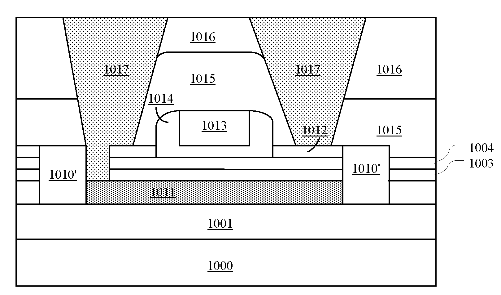
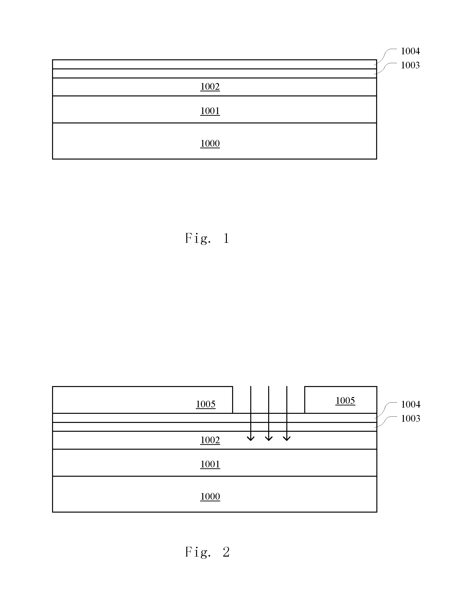
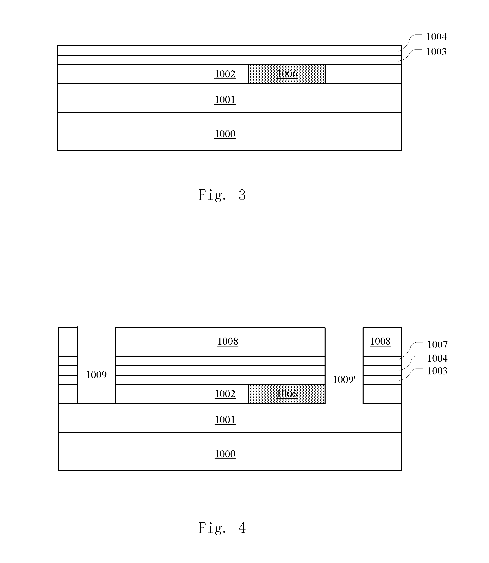
[0056]The embodiments of present invention will be described below in detail in connection with attached drawings. The same reference numerals are used throughout the figures to indicate the same or similar part or the part having the same or similar functions. The embodiments described below in connection with the attached drawings are only illustrative for explaining the present invention, and are not construed as limiting the invention.

[0057]The disclosure below provides various embodiments or examples for carrying out the technical solution of the present invention. Although the parts and arrangements of some specific examples are described, the parts and arrangements are only given as examples, and are not construed as limiting the present invention.

[0058]Moreover, the invention provides various specific processes and / or materials. Nevertheless, one skilled person in the art will appreciate that other processes and / or materials can also be used as alternatives without departing...


PUM


Abstract

The present application discloses a semiconductor structure and a method for manufacturing the same. The semiconductor structure according to the present invention adjusts a threshold voltage with a common contact, which has a portion outside the source or drain region extending to the back-gate region and provides an electrical contact of the source or drain region and the back-gate region, which leads to a simple manufacturing process, an increased integration level and a lowered manufacture cost. Moreover, the asymmetric design of the back-gate structure further increases the threshold voltage and improves the performance of the device.

Description

FIELD OF INVENTION[0001]The present invention relates to semiconductor technology, and more particularly, to a semiconductor-on-insulator (SOI) metal oxide semiconductor field effect transistor (MOSFET) structure and a method for manufacturing the same.DESCRIPTION OF RELATED ART[0002]A complementary metal oxide semiconductor transistor has an increasingly decreasing gate pitch so as to provide improved efficiency and lowered manufacturing cost in very large scale integrated circuits. However, reduction of gate pitch may lead to short channel effects, which deteriorate performance of the device.[0003]In SOI technology, devices and circuits are formed on a silicon film of an insulating layer. Due to the existence of a buried oxide layer, the devices are completely isolated from each other. Thus, the SOI-CMOS integrated circuits intrinsically avoids the latch up effect of a bulk silicon CMOS. Moreover, a fully depleted SOI (FD-SOI) device may form a shallow junction and has a relativel...

Claims


Application Information

Patent Timeline
Patent Type & Authority Applications(United States)
IPC IPC(8): H01L29/772H01L21/336
CPCH01L21/84H01L29/42384H01L29/4908H01L29/6675H01L29/78603H01L2924/0002H01L29/78648H01L2924/00
Inventor ZHU, HUILONGLIANG, QINGQINGYIN, HAIZHOULUO, ZHIJIONG
Owner INST OF MICROELECTRONICS CHINESE ACAD OF SCI
Why Eureka
Try Eureka