Antenna

a technology of antennas and antennas, applied in the field of antennas, can solve the problems of high cost, high radiation efficiency of on-chip antennas, and high cost, and achieve the effect of improving radiation directivity and/or radiation uniformity of antennas

Inactive Publication Date: 2012-05-03
SONY CORP
View PDF9 Cites 9 Cited by
  • Summary
  • Abstract
  • Description
  • Claims
  • Application Information

AI Technical Summary

Benefits of technology

[0010]In general terms the invention proposes a resonant cavity adjacent to one end of a BWA. This may have the advantage that the antenna radiation uniformity and/or the radiation directivity are improved. The side-lobe and other undesired peak of the antenna radiation pattern may be reduced, so the invention may be suitable for dual antenna duplex applications, where two antennas are close to each other and inter-antenna isolation

Problems solved by technology

But this may be complex and high cost.
Also the MMW signal coupling from the IC die to the substrate where the antenna is may cause additional loss.
However the radiation efficiency of an on-chip antenna may be very low due to the high loss tangent of the die.
It is limited to single-ended feeding application and it requires a ground plane

Method used


Image

  • Antenna
  • Antenna
  • Antenna

Examples


Embodiment Construction

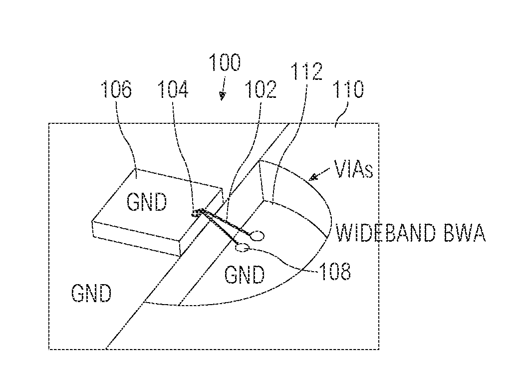
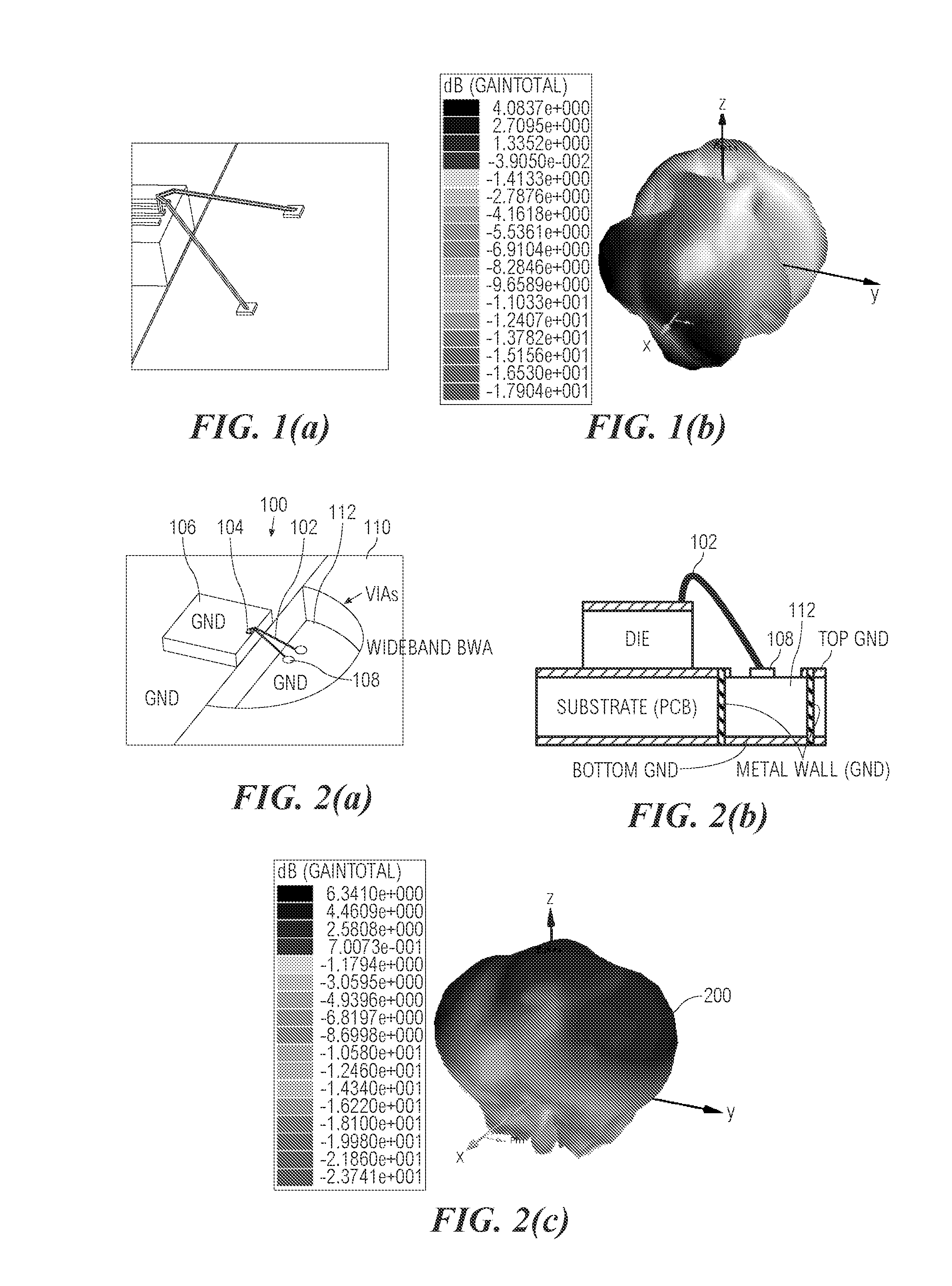
[0038]A cavity BWA 100 according to the example embodiment is shown in FIGS. 2(a) & (b). Two bond-wires 102, which are bonded at same signal port 104 on an IC die 106 and the other ends are bonded at separated bond pads 108 on the substrate 110, respectively, and a cavity 112 just below the bond pads 108. Here, the cavity is defined as 3-dimension dielectric, air or vacuum area surrounded by metal wall except one side open. The cavity 112 can be a substrate integrated cavity [8]. The substrate integrated cavity is made of 2 metal layers sandwiching a dielectric substrate (e.g. printed circuit board: PCB). At the cavity portion, one of the metal layers is etched. The area etched is the aperture of the cavity. Around the edges of the aperture, there is a vertical metal wall. The metal wall can be made of aligned through hole VIAs connecting top and bottom metal layers. The aperture size and the volume of the cavity 112 may depend on the working central frequency wavelength. For exampl...


PUM


Abstract

An antenna including one or more IC bond bands configured to connect to a signal port on an IC, one or more substrate bond pads, a bond wire antenna (BWA) connected between the one or more IC bond bands and the substrate bond pads, and a resonant cavity adjacent the one or more substrate bond pads.

Description

RELATED APPLICATION DATA[0001]The present application claims priority to Singapore Patent Application 201008040-6 filed in the Singapore Patent Office on Oct. 28, 2010, the entire contents of which are hereby incorporated by reference.BACKGROUND OF THE INVENTION[0002]The present invention relates to an antenna particularly though not solely to a bond wire antenna (BWA) for millimetre wave (MMW) signals.[0003]A MMW wave antenna is often made on the printed circuit board (PCB) or other solid substrate. Due to the materials used, the loss tangent in a commercial PCB substrate in the MMW frequency band may be high. To improve efficiency, special processing on low loss material such as miniaturized electromechanical system (MEMS) processing on glass (alumina) may be used. But this may be complex and high cost.[0004]Also the MMW signal coupling from the IC die to the substrate where the antenna is may cause additional loss. The antenna can be directly designed in the IC die (on-chip anten...

Claims


Application Information

Patent Timeline
IPC IPC(8): H01Q1/50
CPCH01L23/66H01L24/49H01L2924/14H01L2924/1461H01L2924/00014H01L2224/49112H01L2224/49109H01L24/48H01L2224/49171H01L2224/48228H01L2224/48227H01L2224/48091H01L2223/6677H01L2223/6611H01Q23/00H01Q1/2283H01L2924/00H01L2224/45099H01L2224/85399H01L2224/05599
Inventor MA, YUGANGSUN, XIAOBINGZHANG, YAQIONG
Owner SONY CORP
Why Eureka
Try Eureka