Insulation sheet made from silicon nitride, and semiconductor module structure using the same

a technology of silicon nitride and silicon nitride, which is applied in the direction of film/foil adhesives, instruments, transportation and packaging, etc., can solve the problems of low thermal conductivity of substrates of about 18 w/mk, insufficient radiation properties, and low strength, and achieve the effect of lowering the thermal radiation properties of the module structur

Active Publication Date: 2012-05-17
KK TOSHIBA +1
View PDF9 Cites 20 Cited by
  • Summary
  • Abstract
  • Description
  • Claims
  • Application Information

AI Technical Summary

Benefits of technology

[0022]When a module structure having a pressure contact structure is formed by using a conventional high thermal-conductivity silicon-nitride substrate which contains β-Si3N4 as a main phase, there has been a problem that a gap is produced between the high thermal-conductivity silicon-nitride substrate and another member such as a pressing member, due to a microscopic unevenness existing on the surface of the high thermal-conductivity silicon-nitride substrate, and the thermal radiation properties of the module structure are lowered.

Problems solved by technology

However, an alumina substrate has the low thermal conductivity of about 18 W / m·K, and accordingly is insufficient in radiation properties.
On the other hand, an AlN substrate has the high thermal conductivity of about 200 W / m·K but has low strength, and accordingly is insufficient in heat-cycle resistance characteristics.
Thus, it is difficult for a conventional alumina substrate or AlN substrate to satisfy the characteristics of both thermal conductivity and strength.
However, in order to manufacture the high thermal-conductivity metal circuit substrate made from silicon nitride described in Patent Documents 1 and 2, a bonding process of bonding the high thermal-conductivity silicon-nitride substrate to the metal circuit board is necessary, which needs a high manufacturing cost.
Because of this, the high thermal-conductivity metal circuit substrate made from silicon nitride needs a high manufacturing cost.
However, it is difficult to eliminate the unevenness even by mirror-polishing the surface to a surface roughness Ra of 0.05 μm or less.
In addition, the mirror polishing also becomes a factor in an increase in manufacturing costs of the high thermal-conductivity silicon-nitride substrate, which is not preferable.
Thus, the high thermal-conductivity silicon-nitride substrate having the microscopic unevenness on the surface has such a problem that a crack tends to be easily formed in the silicon-nitride substrate.
The crack initiates from the salient when the high thermal-conductivity silicon-nitride substrate is used in such a state that a pressure contact stress is applied onto the microscopic unevenness, particularly onto the salient for a long period of time.
In addition, the high thermal-conductivity silicon-nitride substrate having the microscopic unevenness on the surface produces a microscopic gap between the surface of the high thermal-conductivity silicon-nitride substrate and another member, when a module structure such as a semiconductor module structure having the pressure contact structure is formed by bringing the surface of the high thermal-conductivity silicon-nitride substrate into contact with the another member such as a pressing member.
However, the pressing member is generally constituted by a hard material such as a metal, and accordingly, it is difficult to fill the microscopic gap with the material of the member by deforming the shape of the surface of the pressing member side so as to match the unevenness of the surface of the high thermal-conductivity silicon-nitride substrate.
For this reason, if the gap is formed between the surface of the high thermal-conductivity silicon-nitride substrate and the pressing member in the module structure having the pressure contact structure, the gap becomes an obstructive factor in thermal conduction and lowers the radiation characteristics of the module structure.

Method used


Image

  • Insulation sheet made from silicon nitride, and semiconductor module structure using the same
  • Insulation sheet made from silicon nitride, and semiconductor module structure using the same
  • Insulation sheet made from silicon nitride, and semiconductor module structure using the same

Examples


first embodiment

Effect of First Embodiment

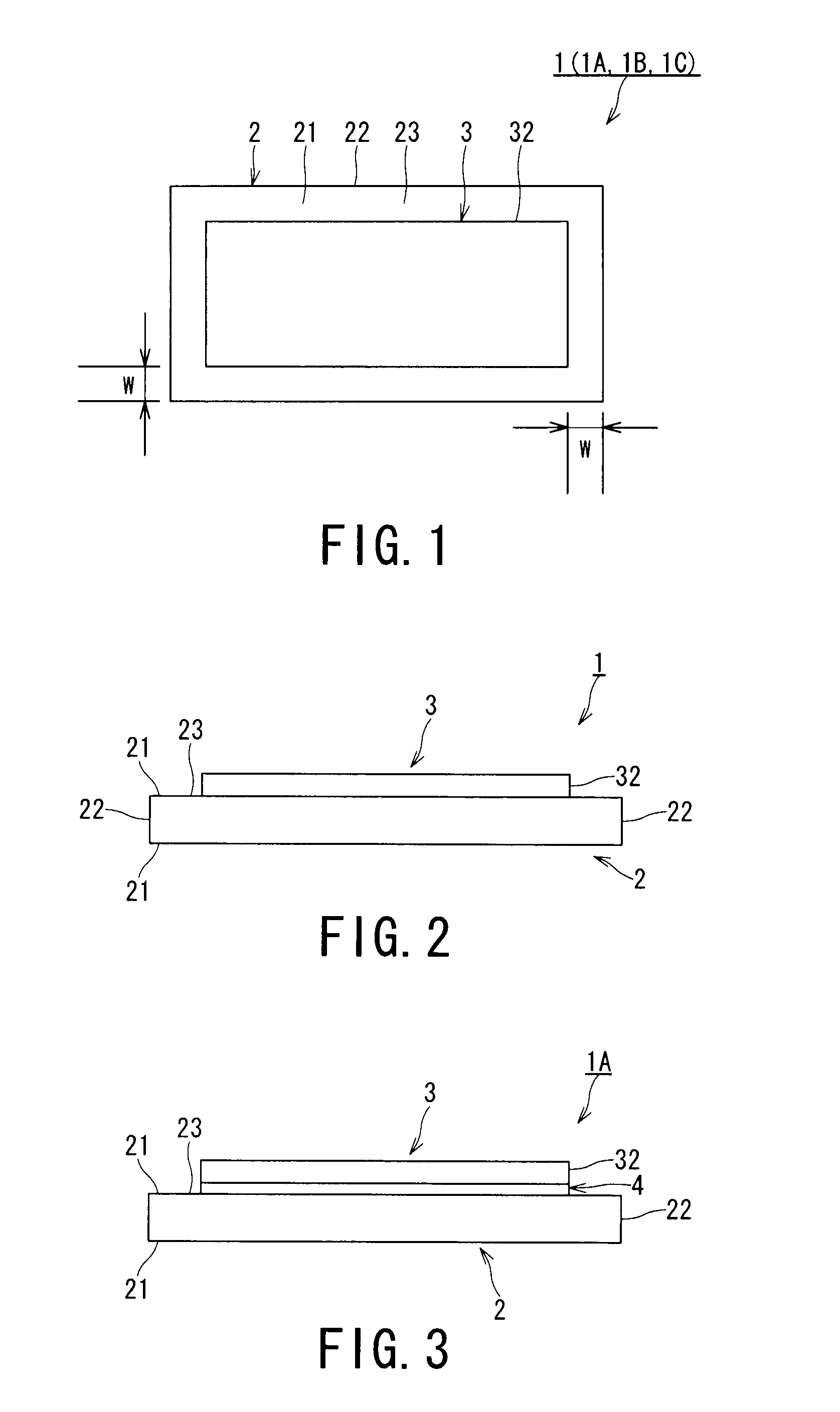
[0123]The insulation sheet 1 made from silicon nitride illustrated as the first embodiment has the surface layer 3 having a predetermined flexibility provided on the surface of the silicon-nitride substrate 2, and accordingly when the insulation sheet 1 made from silicon nitride and the another member such as the pressing member arranged in the surface layer 3 side of the insulation sheet 1 made from silicon nitride are brought into pressure contact with each other, the insulation sheet 1 made from silicon nitride can come in close contact with the another member through the surface layer 3.

[0124]In addition, the insulation sheet 1 made from silicon nitride illustrated as the first embodiment enhances thermal conduction between the insulation sheet 1 made from silicon nitride and another member such as the pressing member, because the insulation sheet 1 made from silicon nitride comes in close contact with the another member such as the pressing member.

[012...

second embodiment

Effect of Second Embodiment

[0141]The insulation sheet 1A made from silicon nitride illustrated as the second embodiment shows a similar effect to that of the insulation sheet 1 made from silicon nitride illustrated as the first embodiment.

[0142]In addition, the insulation sheet 1A made from silicon nitride illustrated as the second embodiment has more enhanced bonding strength between the silicon-nitride substrate 2 and the surface layer 3 in comparison with the insulation sheet 1 made from silicon nitride illustrated as the first embodiment because the reaction layer 4 strongly bonds the surface layer 3 to the silicon-nitride substrate 2.

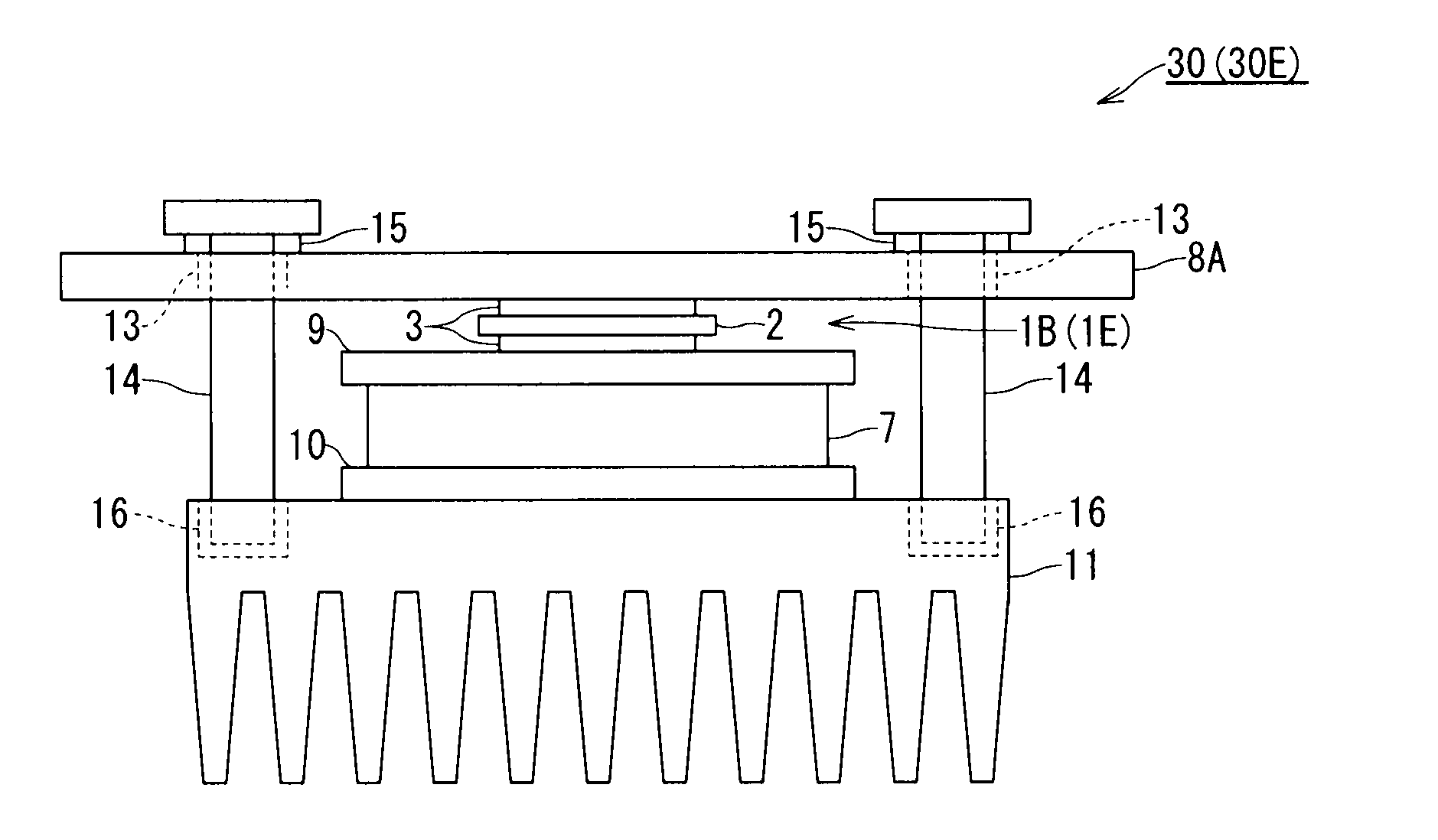
[0143]The insulation sheet 1A made from silicon nitride illustrated as the second embodiment has thus high bonding strength. Accordingly, the insulation sheet 1A can show sufficient durability and thermal radiation properties when being used as the component of the semiconductor module structure having the first pressure contact structure in which ...

third embodiment

Effect of Third Embodiment

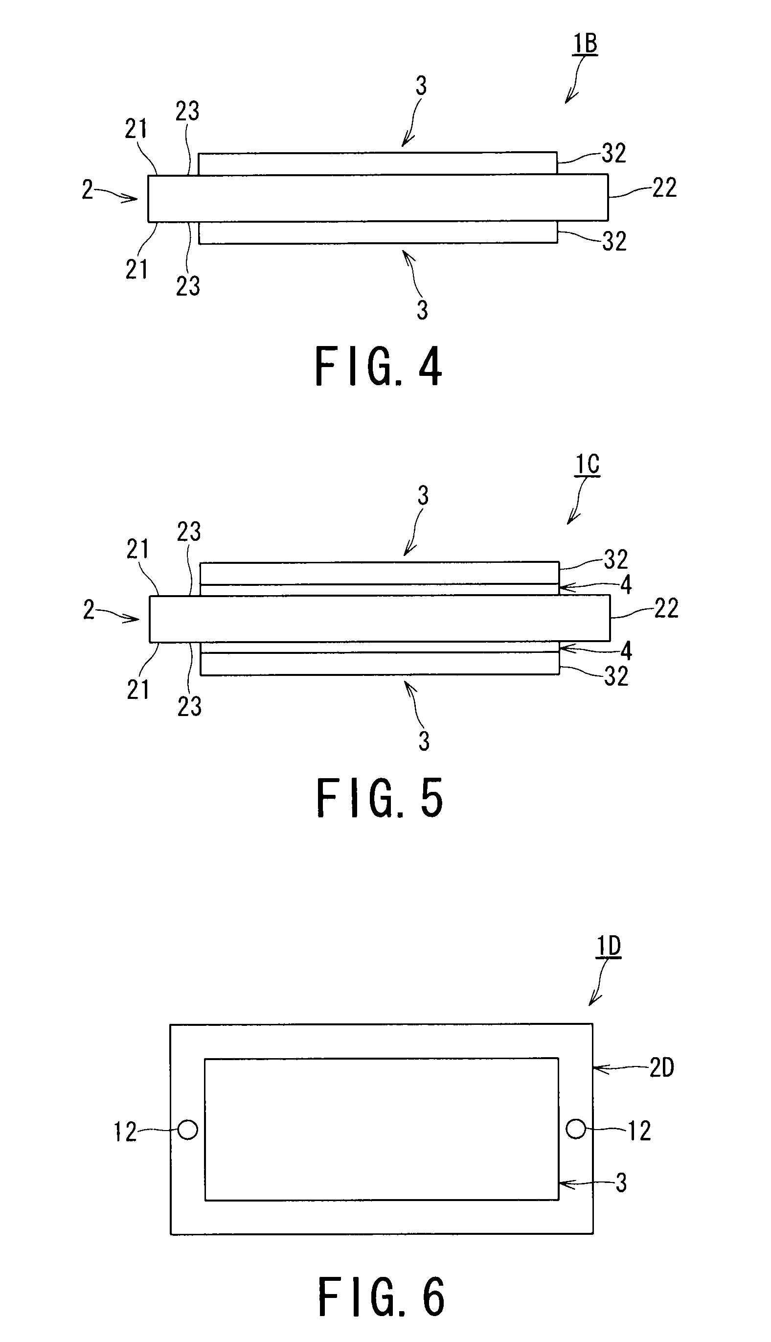
[0148]The insulation sheet 1B made from silicon nitride illustrated as the third embodiment shows a similar effect to that of the insulation sheet 1 made from silicon nitride illustrated as the first embodiment.

[0149]In addition, the insulation sheet 1B made from silicon nitride illustrated as the third embodiment can come in close contact with another member through the surface layers 3 in both front and back face sides of the silicon-nitride substrate 2, in comparison with the insulation sheet 1 made from silicon nitride which is illustrated as the first embodiment and has the surface layer 3 formed only on one face of the silicon-nitride substrate 2, because the insulation sheet 1B has the surface layers 3 formed on both front and back faces of the silicon-nitride substrate 2.

[0150]Furthermore, the insulation sheet 1B made from silicon nitride illustrated as the third embodiment enhances thermal conduction between the insulation sheet 1B made from silico...


PUM

PropertyMeasurementUnit
thicknessaaaaaaaaaa
surface roughness Raaaaaaaaaaa
thicknessaaaaaaaaaa

Abstract

An insulation sheet made from silicon nitride comprising: a sheet-shaped silicon-nitride substrate which contains β-silicon-nitride crystal grains as a main phase; and a surface layer which is formed on one face or both front and back faces of surfaces of the silicon-nitride substrate and is formed from a resin or a metal which includes at least one element selected from among In, Sn, Al, Ag, Au, Cu, Ni, Pb, Pd, Sr, Ce, Fe, Nb, Ta, V and Ti. A semiconductor module structure using the insulation sheet made from silicon nitride.

Description

TECHNICAL FIELD[0001]An embodiment according to the present invention relates to an insulation sheet made from silicon nitride and a semiconductor module structure using the same.BACKGROUND ART[0002]Conventionally, a ceramic metal circuit substrate having an insulation and electrode function has been used in a field of mounting power electronics. The ceramic metal circuit substrate is used as a substrate of a semiconductor module having the insulation and electrode function, for instance, in a semiconductor module structure including a semiconductor module and a radiating member such as a radiation fin. In addition, the semiconductor module structure has been required to have high radiation properties along with the tendency for the power of a semiconductor module to increase in recent years.[0003]In such insulation and electrode fields, a substrate which contains alumina (Al2O3) or aluminum nitride (AlN) as a main component has been conventionally used as a ceramic substrate.[0004]...

Claims


Application Information

Patent Timeline
Patent Type & Authority Applications(United States)
IPC IPC(8): H01L23/04B32B3/00B32B9/04
CPCC04B2111/00844Y10T428/24355C04B2235/786C04B2235/788C04B2235/95C04B2235/96C04B2235/9607C04B2235/963H01L23/15H01L23/3735H01L23/4006C04B2235/767Y10T428/265Y10T428/24802Y10T428/266H01L23/13H01L2924/0002C04B41/88C04B41/83C04B41/5161C04B41/5155C04B41/515C04B41/5127C04B41/5116C04B41/4961C04B41/4853C04B41/009C04B35/584C04B41/4539C04B41/5133C04B41/5063H01L2924/00Y10T428/12472Y10T428/2495Y10T428/259Y10T428/263
Inventor NABA, TAKAYUKI
Owner KK TOSHIBA
Why Eureka
Try Eureka