Analog-to-Digital Converter

a converter and analog technology, applied in the field of analog-to-digital converters, can solve the problems of deteriorating effective resolution, insufficient performance of the technology disclosed in the above-mentioned related-art documents, and difficulty in realizing the resolution of 17 bits or more, and achieve the effect of high conversion rate and high resolution

Inactive Publication Date: 2012-05-31
HITACHI LTD
View PDF7 Cites 13 Cited by
  • Summary
  • Abstract
  • Description
  • Claims
  • Application Information

AI Technical Summary

Benefits of technology

[0016]According to the aspects of the present invention, there can be provided the success...

Problems solved by technology

However, the present inventors have found that the technologies disclosed in the above-mentioned related-art documents are inadequate to perform both of the conversion rate of 1 MS/s or more and the effective resolution of 18 bits or more in the successive approximation ADC.
As a result, a distortion occurs in the A/D conversion result to deteriorate the effective resolution.
As a result of study, even if an MIM (metal insulator metal) capacitor small in the voltage dependence is used, it has been found there is a difficulty in realizing the resolution of 17 bits or more due to the generation of the above third-order distortion component of the sampling charge (the simulation result used in the above study will be d...

Method used


Image

  • Analog-to-Digital Converter
  • Analog-to-Digital Converter
  • Analog-to-Digital Converter

Examples


first embodiment

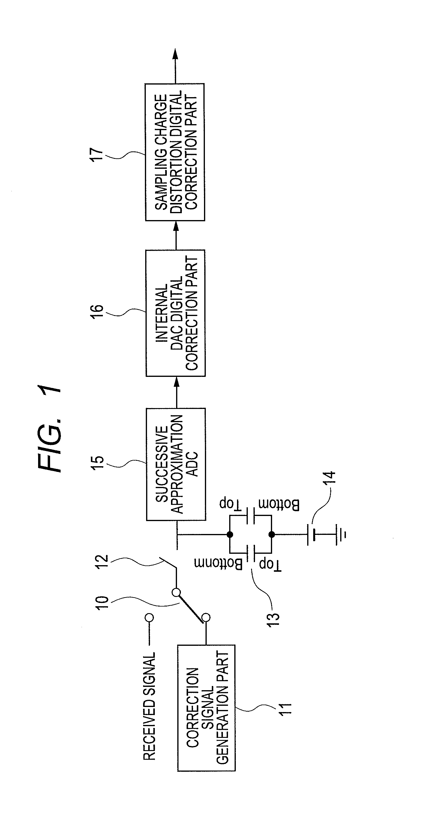
[0036]FIG. 1 illustrates a first embodiment of the present invention. An A / D converter in FIG. 1 includes an input signal changeover switch 10, a sampling part having a sampling switch 12, a sampling capacitor 13, and a bias voltage source 14, a successive approximation A / D conversion part 15, an internal DAC digital correction part 16 connected to a downstream of the successive approximation A / D conversion part 15, a sampling charge distortion digital correction part 17 connected to a downstream of the internal DAC digital correction part 16, and a correction signal generation part 11 that generates a correction signal.

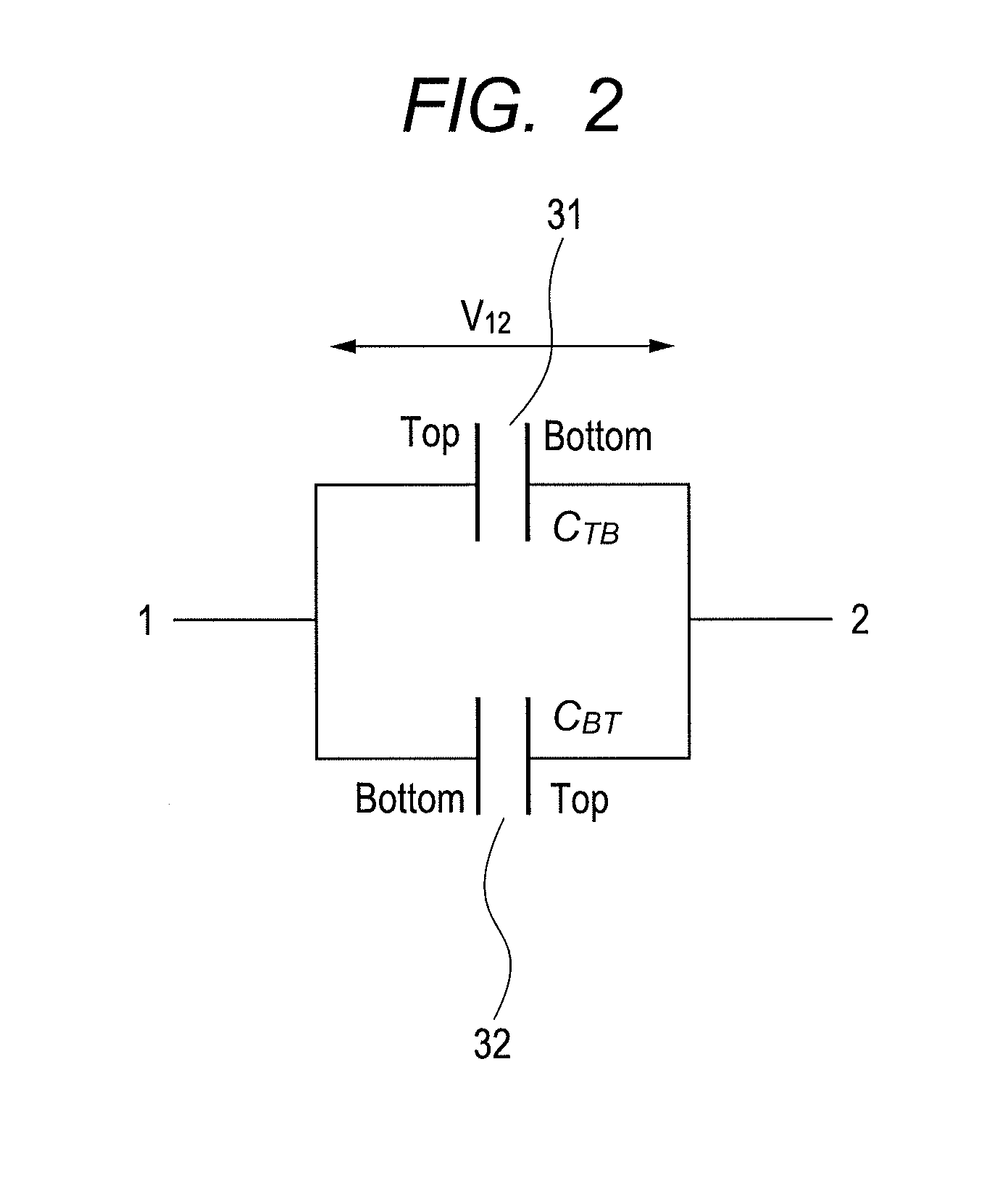
[0037]The successive approximation ADC conducts A / D conversion on charge sampled by the sampling capacitor 13. The sampling capacitor 13 is of a structure in which a first capacitor and a second capacitor each having the same capacitance value are connected in inverse parallel to each other. With this structure, a first-order dependence of the capacitance value on an...

second embodiment

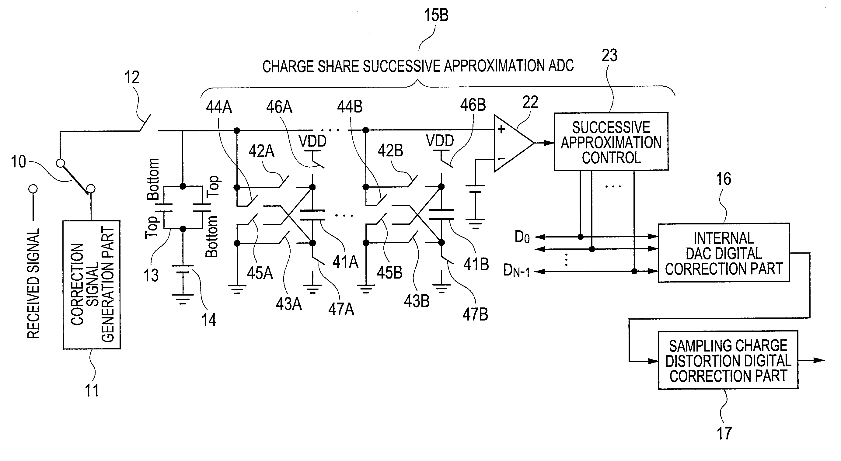
[0053]FIG. 4 illustrates a second embodiment of the present invention. In this embodiment, referring to FIG. 1, the successive approximation A / D conversion part 15 is configured by a charge redistribution successive approximation ADC 15A. In the charge redistribution successive approximation ADC, internal DAC capacitors 21A to 21D also function as the sampling capacitor.

[0054]An A / D converter in FIG. 4 includes the charge redistribution successive approximation ADC 15A which is totally configured by the input signal changeover switch 10, the sampling part having sampling / DAC changeover switches 20A to 20D, internal DAC / sampling capacitors 21A to 21D, the bias voltage source 14, and a reset switch 24, the comparator 22, and the successive approximation control part 23. The A / D converter of FIG. 4 also includes the internal DAC digital correction part 16 connected to a downstream of the charge redistribution successive approximation ADC 15A, the sampling charge distortion digital corr...

third embodiment

[0060]As a third embodiment of the present invention, FIG. 5 illustrates an example of the operation timing. At the time of the digital correction of the internal DAC, the correction signal generation part 11 generates a waveform in which a value is widely changed within an input range of the ADC such as a chopping wave or a sine wave as the internal DAC correction signal, to thereby activate a lookup algorithm of the internal DAC correction factor in the internal DAC digital correction part 16 so that the convergence of the lookup algorithm can be enhanced. Also, at the time of the digital correction of the sampling charge distortion, the correction signal generation part 11 generates DC voltages DC1, DC2, and DC3 having three kinds of voltage values as the sampling charge distortion correction signals. With the use of those DC voltages DC1, DC2, and DC3, the sampling charge distortion digital correction part 17 conducts the digital correction. Specifically, if DC=0 is met, the DC ...


PUM


Abstract

In a successive approximation ADC, resolution is limited because a distortion occurs in an A/D conversion result due to a voltage dependence of a sampling capacitance. An A/D converter includes a sampling capacitor part in which capacitors equal in capacitance value to each other are connected inversely, a successive approximation A/D conversion part that conducts A/D conversion on the sampling charge, a digital correction part that corrects capacitance variation of internal DAC capacitors in the successive approximation A/D conversion part, and a digital correction part that digitally corrects a third-order or more factor of a voltage dependence of the sampling charge.

Description

CLAIM OF PRIORITY[0001]The present application claims priority from Japanese patent application JP 2010-263076 filed on Nov. 26, 2010, the content of which is hereby incorporated by reference into this application.FIELD OF THE INVENTION[0002]The present invention relates to an analog-to-digital converter that conducts digital correction.BACKGROUND OF THE INVENTION[0003]In next-generation high-definition medical diagnostic imaging devices, there is required an analog-to-digital converter that can realize an extremely high effective resolution of 18 bits or more at a conversion rate of 1 MS / s or higher. As such an ultrahigh resolution ADC, a sigma-delta ADC and a successive approximation ADC have been known.[0004]In the case of the sigma-delta ADC, with employment of an internal quantizer of 1 bit, there is no need to provide a precision in an analog circuit. Also, with an increase in an internal operation clock frequency, a high effective resolution of 20 bits or more can be realized...

Claims


Application Information

Patent Timeline
IPC IPC(8): H03M1/38H03M1/06
CPCH03M1/068H03M1/468H03M1/1052
Inventor OSHIMA, TAKASHI
Owner HITACHI LTD
Why Eureka
Try Eureka