
Thin film transistor substrate and method for manufacturing the same

Active Publication Date: 2012-06-07
LG DISPLAY CO LTD
View PDF3 Cites 12 Cited by
  • Summary
  • Abstract
  • Description
  • Claims
  • Application Information

AI Technical Summary

Benefits of technology

[0024]An advantage of the present invention is to provide a thin film transistor substrate and a method for manufacturing the same in which a gate electrode is formed at a thin thickness to prevent a crack from occurring in a gate insulating film formed on the gate electrode when a laser is irradiated and improve on current characteristics of a thin film transistor without increasing resistance of the gate electrode.
[0025]Additional advantages and features of the invention will be set forth in part in the description which follows and in part will become apparent to those having ordinary skill in the art upon examination of the following or may be learned from practice of the invention. The objectives and other advantages of the invention may be realized and attained by the structure particularly pointed out in the written description and claims hereof as well as the appended drawings.
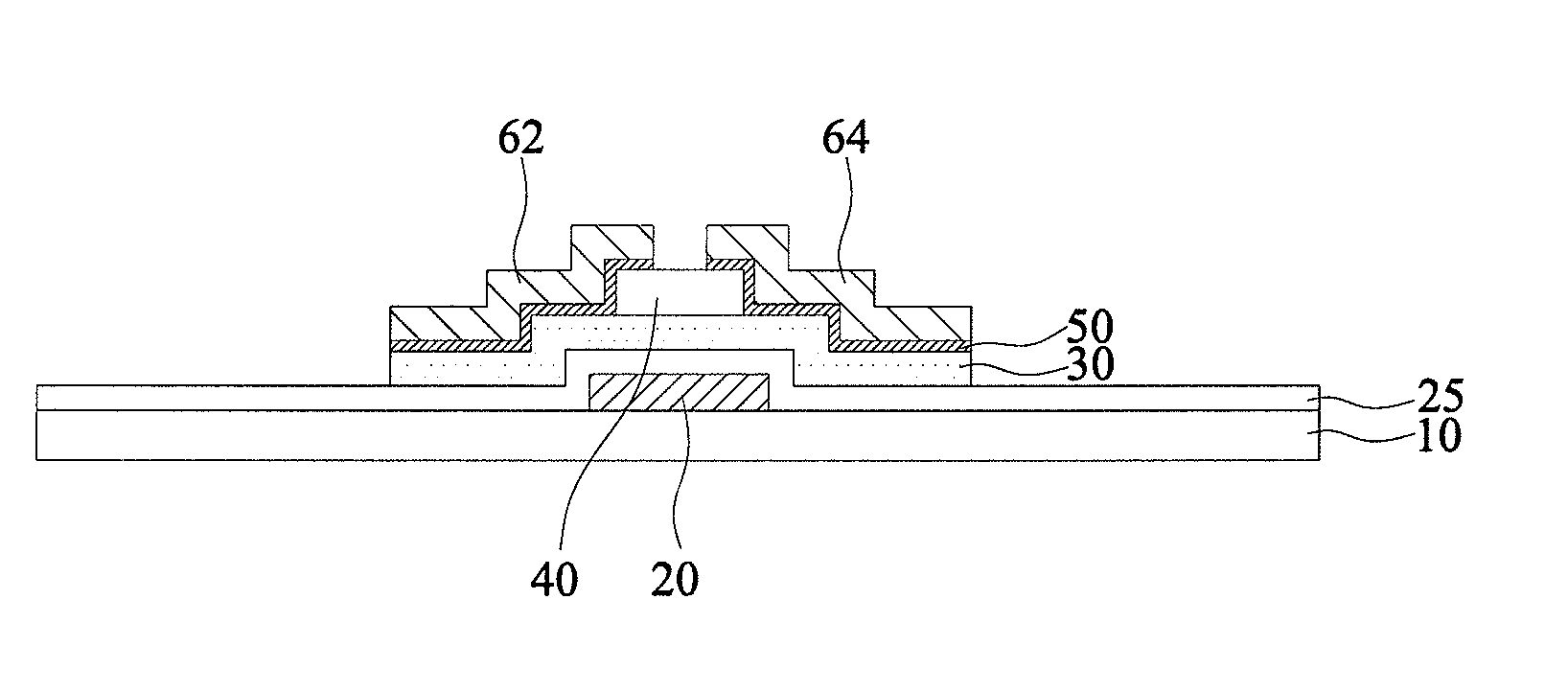
[0026]To achieve these objects and other advantages and in accordance with the purpose of the invention, as embodied and broadly described herein, a thin film transistor substrate comprises a gate line and a data line arranged on a substrate to cross each other; a gate electrode connected with the gate line below the gate line; an active layer formed on the gate electrode; an etch stopper formed on the active layer; an ohmic contact layer formed on the etch stopper; source and drain electrodes formed on the ohmic contact layer; and a pixel electrode connected with the drain electrode.
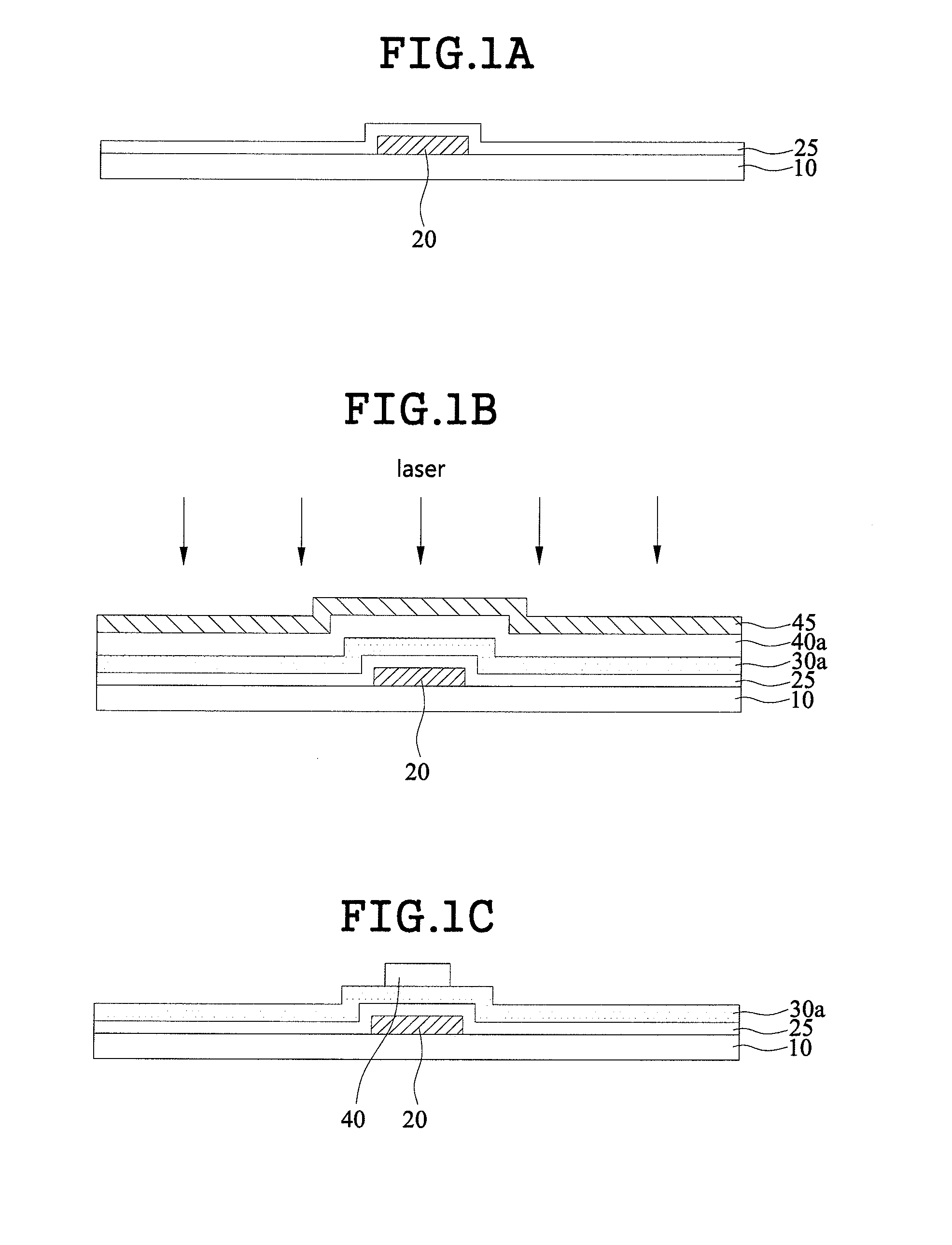
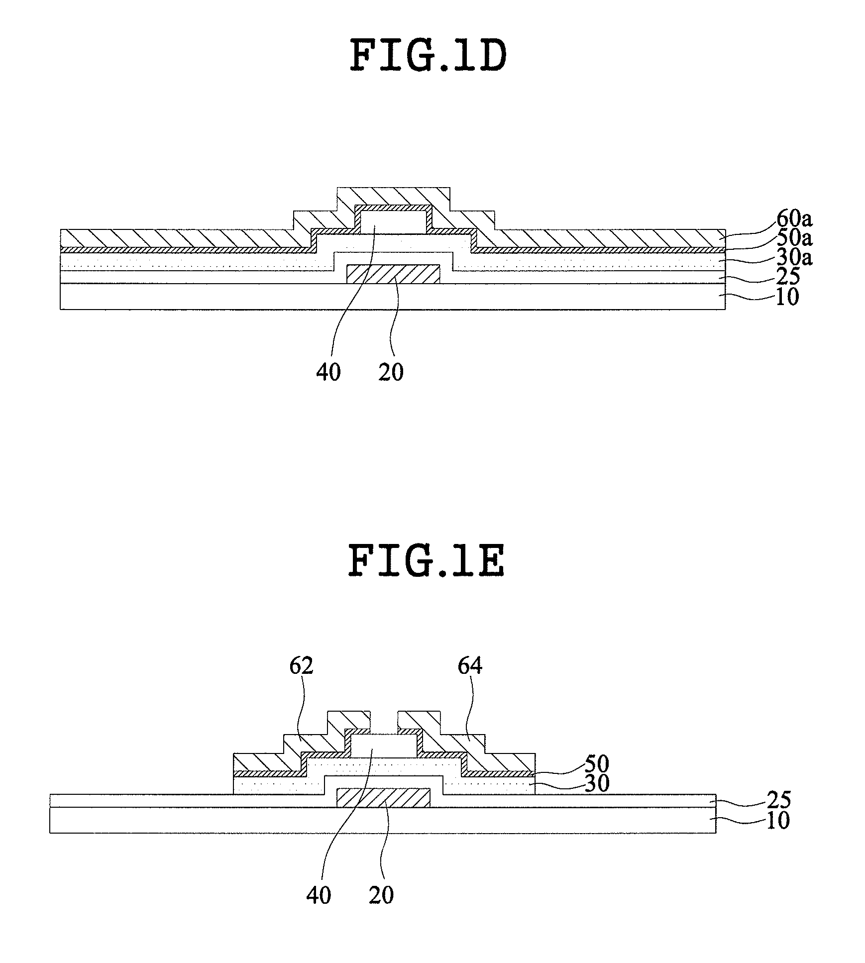
[0027]In another aspect of the present invention, a method for manufacturing a thin film transistor substrate comprises the steps of forming a gate electrode on a substrate and forming a gate line on the gate electrode; forming a gate insulating film on the gate line, forming an active layer on the gate insulating film, and forming an etch stopper layer on the active layer; forming a heat transfer layer on the etch stopper layer and crystallizing the active layer by irradiating a laser; removing the heat transfer layer after etching the etch stopper layer using the heat transfer layer as a mask; forming an ohmic contact layer on an entire surface of the substrate including the etch stopper layer and forming a source / drain electrode layer on the ohmic contact layer; patterning the active layer, the etch stopper layer, the ohmic contact layer and the source / drain electrode layer to form the active layer, an etch stopper, the ohmic contact layer, a source electrode and a drain electrode at predetermined patterns; and forming a pixel electrode connected with the drain electrode after forming a passivation film on the entire surface of the substrate including the source electrode and the drain electrode.

Problems solved by technology

In the back channel etched type thin film transistor, a channel region of a semiconductor layer is etched during an etching process for forming the source and drain electrodes, and in this case, a problem occurs in that the active layer may be too etched.
However, the aforementioned thin film transistor according to the related art has the following problems.
However, in this case, problems occur in that resistance of the gate electrode 20 increases and on current characteristics of the thin film transistor may be deteriorated.

Method used


Image

  • Thin film transistor substrate and method for manufacturing the same
  • Thin film transistor substrate and method for manufacturing the same
  • Thin film transistor substrate and method for manufacturing the same

Examples


first embodiment

[0036]FIG. 2A is a plane view illustrating a thin film transistor substrate according to the present invention and FIG. 2B is a cross-sectional view taken along line I-I of FIG. 2A.

[0037]As shown in FIG. 2A, a gate line 120 and a data line 170 are formed on a substrate 100 to cross each other.

[0038]A gate electrode 110 is connected to the gate line 120. The gate electrode 110 is formed at a layer different from the gate line 120, more specifically below the gate line 120.

[0039]A source electrode 172 is connected to the data line 170, and a drain electrode 174 is formed to face the source electrode 172 and spaced apart from the source electrode 172 at a predetermined interval. The source electrode 172 is forked from the data line 170.

[0040]Since an etch stopper 150 is formed at a channel region where the source electrode 172 and the drain electrode 174 are spaced apart from each other, an active layer formed below the etch stopper 150 is prevented from being etched.

[0041]A pixel elec...

second embodiment

[0084]FIG. 4A is a plane view illustrating a thin film transistor substrate according to the present invention and FIG. 4B is a cross-sectional view taken along line I-I of FIG. 4A.

[0085]As shown in FIG. 4A, a gate line 120 and a data line 170 are formed on a substrate 100 to cross each other.

[0086]A gate electrode 110 is connected to the gate line 120, and is formed below the gate line 120.

[0087]A source electrode 172 is connected to the data line 170, and a drain electrode 174 is formed to face the source electrode 172 and spaced apart from the source electrode 172 at a predetermined interval. The source electrode 172 is forked from the data line 170.

[0088]An etch stopper 150 is formed at a channel region where the source electrode 172 and the drain electrode 174 are spaced apart from each other.

[0089]The etch stopper 150 is formed below the source electrode 172 and the drain electrode 174 at the same width W as the widths of the source electrode 172 and the drain electrode 174. A...


PUM


Abstract

A thin film transistor substrate and a method for manufacturing the same are discussed, in which the thin film transistor comprises a gate line and a data line arranged on a substrate to cross each other; a gate electrode connected with the gate line below the gate line; an active layer formed on the gate electrode; an etch stopper formed on the active layer; an ohmic contact layer formed on the etch stopper; source and drain electrodes formed on the ohmic contact layer; and a pixel electrode connected with the drain electrode. It is possible to prevent a crack from occurring in the gate insulating film during irradiation of the laser and prevent resistance of the gate electrode from being increased.

Description

CROSS REFERENCE TO RELATED APPLICATIONS[0001]This application claims the benefit of the Korean Patent Application No. 10-2010-0123715 filed on Dec. 6, 2010, which is hereby incorporated by reference for all purposes as if fully set forth herein.BACKGROUND OF THE INVENTION[0002]1. Field of the Invention[0003]The present invention relates to a thin film transistor substrate that can be applied to a display device such as a liquid crystal display device, and more particularly, to a thin film transistor that crystallizes an active layer by using a laser.[0004]2. Discussion of the Related Art[0005]A thin film transistor has been widely used as a switching device of a display device such as a liquid crystal display device.[0006]The thin film transistor includes a gate electrode, an active layer, and source and drain electrodes, and may be divided into a staggered structure and a coplanar structure depending on arrangement of the electrodes.[0007]In the staggered structure, the gate electr...

Claims


Application Information

Patent Timeline
IPC IPC(8): H01L29/786H01L21/336
CPCH01L27/124H01L27/1281H01L29/66765H01L21/02675H01L27/1288H01L29/42384
Inventor KIM, KITAE
Owner LG DISPLAY CO LTD
Learn More