Liquid crystal display panel
a liquid crystal display and panel technology, applied in the field of liquid crystal display panels, can solve the problems of slow response time, negative influence on the other parameters of the lc cell, and inability to achieve all these requirements at the same time, and achieve excellent contrast ratio, display characteristics, and viewing angle characteristics.
- Summary
- Abstract
- Description
- Claims
- Application Information
AI Technical Summary
Benefits of technology
Problems solved by technology
Method used
Image
Examples
embodiment 1
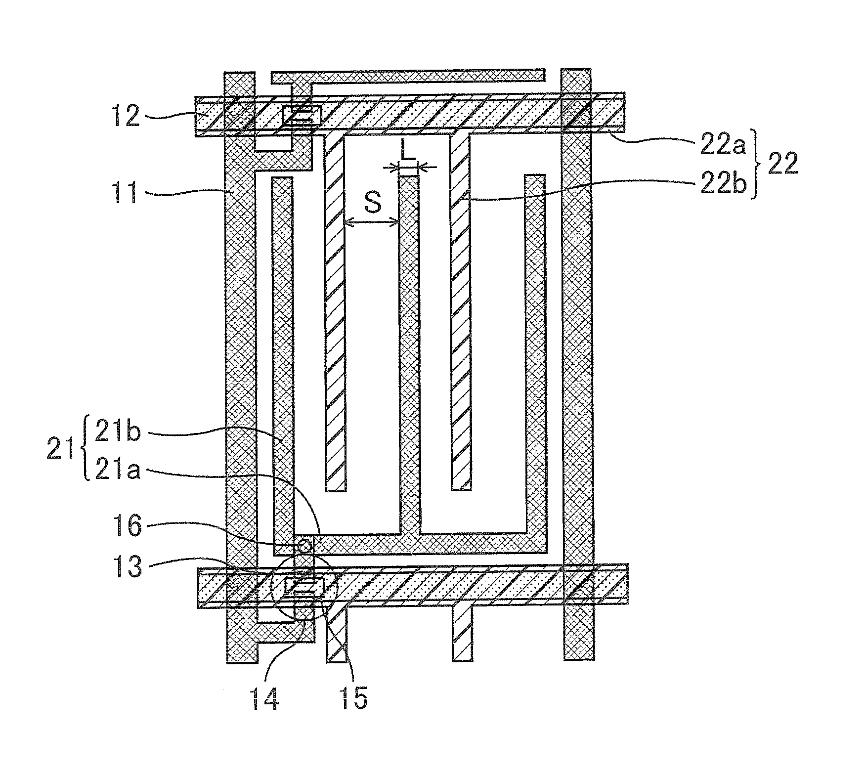
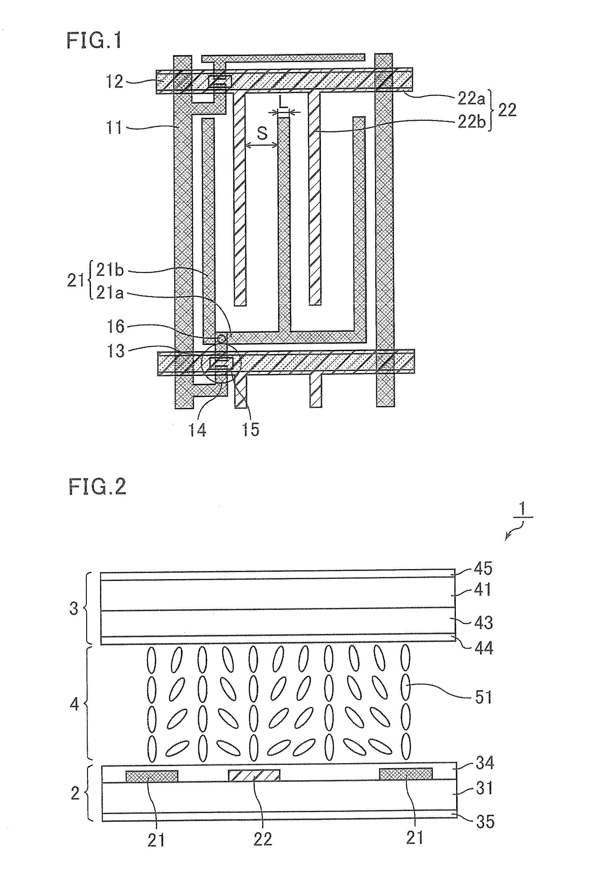
[0077]The LCD panel of Embodiment 1 is a TEA-LCD panel where a pair of electrodes provided in the same substrate forms an arch-like lateral electric field in an LC medium and the alignment of LC molecules whose initial alignment is vertical alignment is controlled, thereby controlling image display.
[0078]According to the LCD panel of Embodiment 1, a plurality of pixels each constituted by a plurality of sub-pixels are arranged in a matrix pattern. The LCD panel of Embodiment 1 includes a pair of substrates composed of a TFT substrate and a counter substrate, and an LC medium interposed therebetween. More specifically, the LCD panel of Embodiment 1 includes these members in order of the TFT substrate, the LCD medium, and the counter substrate from the back face side to the observation face side. The LC medium contains nematic LCs with positive dielectric anisotropy (Δ∈>0).
[0079]FIG. 1 is a plan view schematically illustrating a configuration per sub-pixel in a TFT substrate of the LC...
example 1
[0131]
CCQU-3-F 9.00%Clearing point [° C.]:94.5CCQU-5-F 9.00%Δn [589 nm, 20° C.]:0.1214PUQU-3-F16.00%Δε[1 kHz, 20° C.]:+20.4APUQU-2-F 8.00%γ1[mPa · s]184APUQU-3-F 9.00%V0[V, 20° C.]:0.81PGUQU-3-F 8.00%CPGU-3-OT 7.00%CC-4-V18.00%CC-5-V 5.00%CCP-V-1 6.00%CCPC-33 3.00%PPGU-3-F 2.00%
embodiment 2
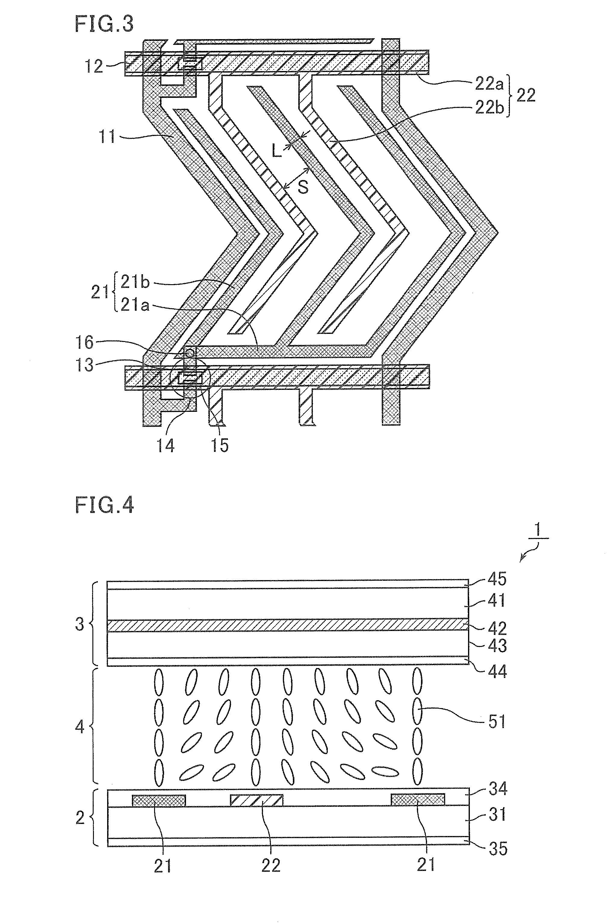
[0132]FIG. 3 is a plan view schematically illustrating a configuration per sub-pixel of a TFT substrate of an LCD panel in Embodiment 2. The LCD panel in Embodiment 2 is the same as that in Embodiment 1, except that the source line 11, the branched part 21b of the pixel electrode 21, and the branched part 22b of the common electrode 22 are each formed not in a linear pattern but in a V pattern per sub-pixel. Further, the source line 11, which is formed over a plurality of sub-pixels, forms a zig-zag pattern in the entire substrate plane. In Embodiment 2, the pair of polarizers is disposed such that the azimuths of their polarization axes are in the same relationship as in Embodiment 1, specifically, in parallel or orthogonal to the extending direction of the gate lines 12.
[0133]The above-mentioned V-shaped part has such a shape as extending two opposite directions from the line bisecting the longitudinal side of the sub-pixel, and the portion extending to one direction and the porti...
PUM
| Property | Measurement | Unit |
|---|---|---|
| width | aaaaa | aaaaa |
| angle | aaaaa | aaaaa |
| temperature | aaaaa | aaaaa |
Abstract
Description
Claims
Application Information


