
Method of applying phosphor to semiconductor light-emitting device

a technology of light-emitting devices and phosphors, which is applied in the testing/measurement of individual semiconductor devices, semiconductor/solid-state devices, instruments, etc., can solve the problems of small size and light weight of semiconductor light-emitting devices, and achieve the effect of increasing the yield rate of white light-emitting device chips and uniform color characteristics

Inactive Publication Date: 2012-06-07
SAMSUNG ELECTRONICS CO LTD
View PDF3 Cites 39 Cited by
  • Summary
  • Abstract
  • Description
  • Claims
  • Application Information

AI Technical Summary

Benefits of technology

[0008]Provided are methods of applying a phosphor to a semiconductor light-emitting device, whereby a uniform color characteristic may be achieved, and a yield rate of manufacture with respect to a white light-emitting device chip may be increased.
[0021]The masking member may function to prevent the phosphor from being applied to electrode pads and areas by masking the electrode pads formed on the top surfaces of the plurality of light-emitting devices, and the areas between the plurality of light-emitting devices.

Problems solved by technology

Also, the semiconductor light-emitting device is excellent in its fast response speed and shock resistance, and furthermore, the semiconductor light-emitting device may be small and lightweight.
However, the wafer level coating technique may be used only for a structure in which light is emitted above the light-emitting devices.

Method used


Image

  • Method of applying phosphor to semiconductor light-emitting device
  • Method of applying phosphor to semiconductor light-emitting device
  • Method of applying phosphor to semiconductor light-emitting device

Examples


Embodiment Construction

[0068]Reference will now be made in detail to embodiments, examples of which are illustrated in the accompanying drawings, wherein like reference numerals refer to the like elements throughout and the size of each component may be exaggerated for clarity. In this regard, the present embodiments may have different forms and should not be construed as being limited to the descriptions set forth herein. Accordingly, the embodiments are merely described below, by referring to the figures, to explain aspects of the present description.

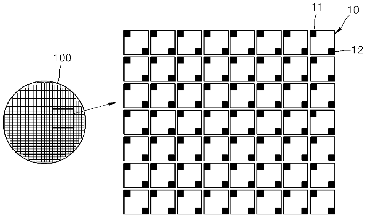
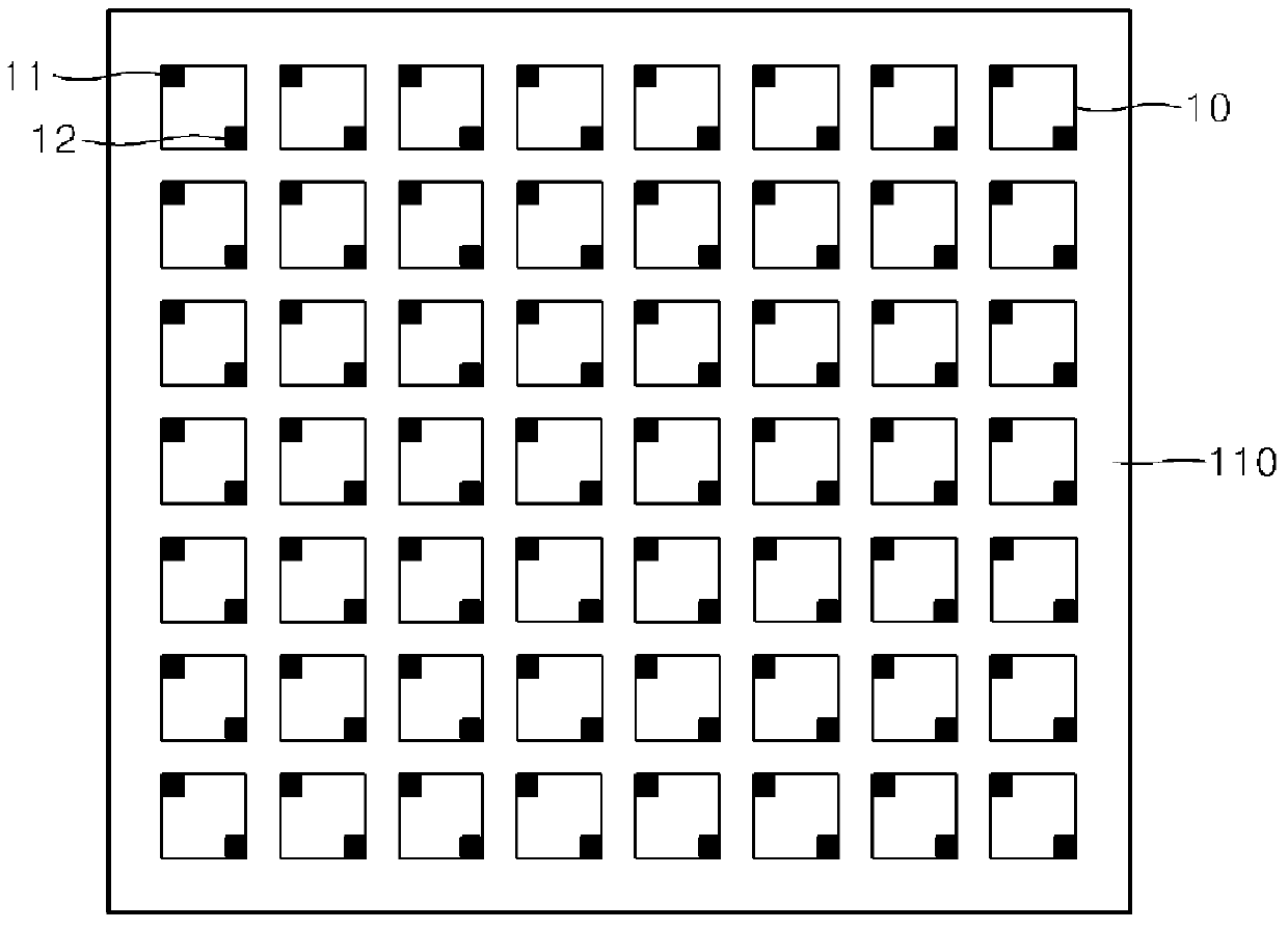
[0069]FIG. 1 illustrates a pattern of a plurality of semiconductor light-emitting device chips 10 formed on a wafer substrate 100 including sapphire. As illustrated in FIG. 1, in general, the semiconductor light-emitting device chips 10 may be arrayed in a rectangular-shape lattice on the wafer substrate 100. The semiconductor light-emitting device chips 10 may be formed on the wafer substrate 100 by performing, but not limited thereto, one of well-known pr...


PUM


Abstract

A method of applying a phosphor according to a light-emission characteristic of semiconductor light-emitting devices so as to increase a yield rate of manufacture with respect to a white light-emitting device chip, the method including the operations of testing light-emission characteristics of a plurality of light-emitting devices formed on a wafer; disposing a plurality of light-emitting devices having the same light-emission characteristics on a carrier substrate; applying a same phosphor to the plurality of light-emitting devices disposed on the carrier substrate; and separating the plurality of arrayed light-emitting devices. Thus, a white light-emitting device chip manufactured by using the method may emit almost the same white light.

Description

CROSS-REFERENCE TO RELATED APPLICATIONS[0001]This application claims the benefit of Korean Patent Application No. 10-2010-0122674, filed on Dec. 3, 2010, in the Korean Intellectual Property Office, the disclosure of which is incorporated herein in its entirety by reference.BACKGROUND[0002]1. Field[0003]The present disclosure relates to methods of applying a phosphor to a semiconductor light-emitting device, and more particularly, to methods of applying a phosphor according to a light-emission characteristic of semiconductor light-emitting devices so as to increase a yield rate of manufacture with respect to a white light-emitting device chip.[0004]2. Description of the Related Art[0005]A light-emitting diode (LED) is a semiconductor light-emitting device that converts an electrical signal into light by using a characteristic of a compound semiconductor. The semiconductor light-emitting device such as the LED is characterized in that a lifetime of the semiconductor light-emitting dev...

Claims


Application Information

Patent Timeline
Patent Type & Authority Applications(United States)
IPC IPC(8): H01L33/08
CPCH01L33/50H01L33/0095
Inventor YOO, CHEOL-JUNHONG, SEONG-JAE
Owner SAMSUNG ELECTRONICS CO LTD
Features
  • Generate Ideas
  • Intellectual Property
  • Life Sciences
  • Materials
  • Tech Scout
  • Unparalleled Data Quality
  • Higher Quality Content
  • 60% Fewer Hallucinations
Learn More