High performance design rule checking technique

a design rule and high-performance technology, applied in the field of electronic design automation, can solve the problems of laborious process, inability to work with analog, rf and custom circuit designs, and increase in the number of rules, and achieve the effect of simplifying the process of creating design rules and reducing the number of rules

Active Publication Date: 2012-06-07
SYNOPSYS INC
View PDF0 Cites 20 Cited by
  • Summary
  • Abstract
  • Description
  • Claims
  • Application Information

AI Technical Summary

Benefits of technology

[0021]A need therefore exists for a robust solution to the problem of rapid checking of design rules during a layout editing process.

Problems solved by technology

The increase in the number of rules has complicated the task of creating design rule clean layouts, i.e., layouts that do not have design rule violations.
Unfortunately, this approach usually does not work for analog, RF and custom circuit designs.
Layouts for such designs are typically created manually using layout editors, and because of the number and complexity of the design rules, checking them was a laborious process.
On the other hand, it can be seen that checking even simple design rules like those above is extremely expensive computationally.
Even then they often can require hours to complete.
The conventional approach also suffers from roughly linear growth of the total run time with respect to the number of rules to be checked, with multiple values for a rule counted as separate rules.
This makes it very hard to reduce the total run time without turning off selected rules.
The conventional approach also suffers from linear growth of run time for individual rule checks, with respect to the length of the geometry operation sequence, i.e., the complexity of the rule.
While some layout editors are able to do this, the checking can be sluggish and usually works only when some of the design rules are turned off.

Method used


Image

  • High performance design rule checking technique
  • High performance design rule checking technique
  • High performance design rule checking technique

Examples


example implementation

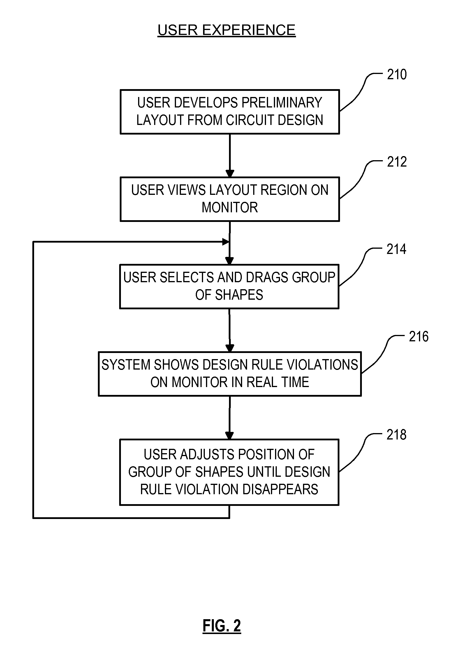
[0059]FIG. 2 illustrates an example user experience when using an embodiment of the system as described herein. The flow chart of FIG. 2 occurs within step 122 (FIG. 1).

[0060]In step 210, the user develops a preliminary layout from a circuit design. As used herein, the term “circuit design” refers to the gate or transistor level design, before layout. The circuit design is often represented internally to the system in a netlist file. The layout is represented internally to the system in a geometry file which defines, among other things, all the shapes to be formed on each mask that will be used to expose the wafer during fabrication. The geometry file can have any of several standard formats, such as GDSII, OASIS, CREF, and so on, or it can have a non-standard format. The file describes the layout of the circuit design in the form of a mask definition for each of the masks to be generated. Each mask definition defines a plurality of polygons. At the time if FIG. 2, no resolution enh...


PUM


Abstract

Roughly described, a design rule data set is developed offline from the design rules of a target fabrication process. A design rule checking method involves traversing the corners of shapes in a layout region, and for each corner, populating a layout topology database with values that depend on respective corner locations. After the layout topology database is populated, the values are compared to values in the design rule data set to detect any design rule violations. Violations can be reported in real time, while the user is manually editing the layout. Preferably corner traversal is performed using scan lines oriented perpendicularly to edge orientations, and scanning in the direction of the edge orientations. Scans stop only at corner positions and populate the layout topology database with what information can be gleaned based on the current scan line. The different scans need not reach each corner simultaneously.

Description

BACKGROUND[0001]The invention relates to electronic design automation, and more particularly, to methods and apparatuses for rapid checking of design rules in a circuit layout.[0002]Advancements in process technology have impacted integrated circuit manufacturing in at least two key ways. First, scaling of device geometry achieved through sub-wavelength lithography has facilitated packing more devices on a chip. Second, different process recipes have enabled manufacturing of heterogeneous devices with different threshold and supply voltages on the same die. A consequence of these improvements, however, has been an explosion in the number of design rules that need to be obeyed in the layout. Instead of simple width and spacing rules, modern fabrication technologies prescribe complex contextual rules that have to be obeyed for manufacturability.[0003]The increase in the number of rules has complicated the task of creating design rule clean layouts, i.e., layouts that do not have desig...

Claims


Application Information

Patent Timeline
Patent Type & Authority Applications(United States)
IPC IPC(8): G06F17/50
CPCG06F2217/06G06F17/5081G06F30/398G06F2111/04
Inventor DAI, ZUOLIU, DICKSU, MING
Owner SYNOPSYS INC
Why Eureka
Try Eureka