High-quality non-polar/semi-polar semiconductor element on an unevenly patterned substrate and a production method therefor

Active Publication Date: 2012-06-21
SEOUL VIOSYS CO LTD +1
View PDF12 Cites 8 Cited by
  • Summary
  • Abstract
  • Description
  • Claims
  • Application Information

AI Technical Summary

Benefits of technology

[0017]According to the semiconductor device and the manufacturing method thereof set forth above, the sapphire crystal plane, which enables the growth of the non-polar/semi-polar nitride semiconductor layer, is etched to form uneven patterns, and the template layer is

Problems solved by technology

However, crystal defects, such as a line defect and a point defect, may be caused by a lattice mismatch between sapphire, which is suitable for the formation of a template layer using non-polar/semi-polar GaN or the like, and a non-polar/semi-polar nitride semiconductor template layer, which is formed on the sapphire, and a difference in coefficient of thermal expansion between constituent elements.
Such crystal defects have a bad influence on the reliability of an optical device, for example, a resistance to electrostatic disc

Method used


Image

  • High-quality non-polar/semi-polar semiconductor element on an unevenly patterned substrate and a production method therefor
  • High-quality non-polar/semi-polar semiconductor element on an unevenly patterned substrate and a production method therefor
  • High-quality non-polar/semi-polar semiconductor element on an unevenly patterned substrate and a production method therefor

Examples


Embodiment Construction

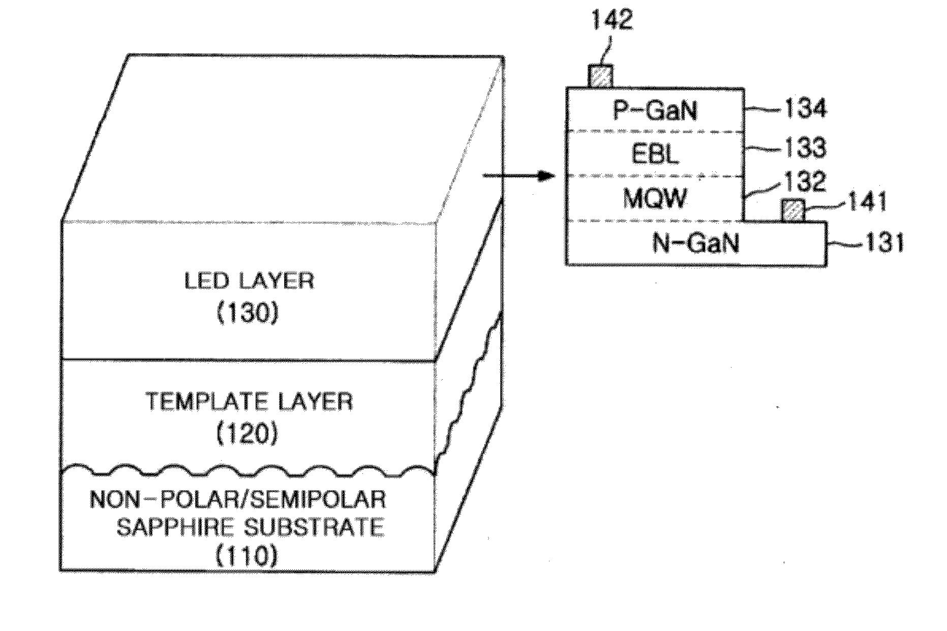
[0029]Exemplary embodiments of the present invention will be described below in detail with reference to the accompanying drawings. These embodiments are provided so that this disclosure will be thorough and complete, and will fully convey the scope of the invention to those skilled in the art. The invention may, however, be embodied in many different forms and should not be construed as being limited to the embodiments set forth herein. Throughout the drawings and description, like reference numerals will be used to refer to like elements.

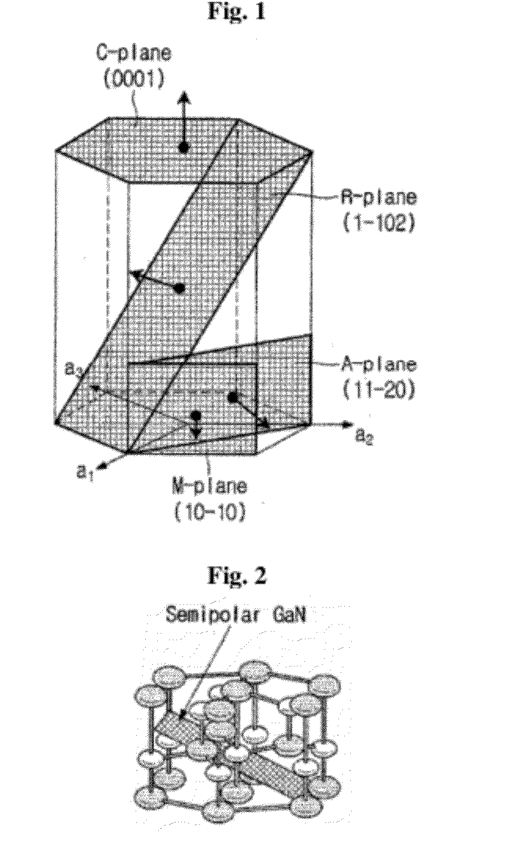
[0030]FIG. 1 illustrates a sapphire crystal structure for explaining a crystal plane of a sapphire substrate.

[0031]In general, if a nitride semiconductor, such as polar GaN, is grown on a sapphire substrate using a C-plane (e.g., (0001) plane) as a sapphire crystal plane, as illustrated in FIG. 1, the internal quantum efficiency may be reduced by a piezoelectric effect caused by the formation of a polarization field.

[0032]In an embodiment of the p...


PUM


Abstract

Provided are a high-quality non-polar/semi-polar semiconductor device with reduced defect density and improved internal quantum efficiency and light extraction efficiency, and a manufacturing method thereof. The manufacturing method is a method for manufacturing a semiconductor device, in which a template layer and a semiconductor device structure are formed on a sapphire substrate having a crystal plane for growing a non-polar or semi-polar nitride semiconductor layer. The sapphire substrate is etched to form uneven patterns, and the template layer including a nitride semiconductor layer and a GaN layer is formed on the sapphire substrate in which the uneven patterns are formed.

Description

CROSS-REFERENCE TO RELATED APPLICATIONS[0001]This application is the National Stage of International Application PCT / KR2010 / 005763, filed on Aug. 27, 2010, and which claims priority from and the benefit of Korean Patent Application No. 10-2009-0080058, filed on Aug. 27, 2009, both of which are herein incorporated by reference for all purposes as if fully set forth herein.BACKGROUND OF THE INVENTION[0002]1. Field of the Invention[0003]The present invention relates to a semiconductor device and a manufacturing method thereof, and more particularly, to a high-quality non-polar / semi-polar semiconductor device and a manufacturing method thereof. In the high-quality non-polar / semi-polar semiconductor device, a non-polar / semi-polar nitride semiconductor crystal is formed on a sapphire crystal plane, which enables the growth of a non-polar / semi-polar nitride semiconductor layer, in order that a piezoelectric effect generated in a polar nitride semiconductor layer may not occur in a nitride ...

Claims


Application Information

Patent Timeline
IPC IPC(8): H01L33/06H01L29/201H01L21/302H01L33/32
CPCH01L33/0062H01L33/20H01L33/16
Inventor NAM, OK HYUNYOO, GEUN HO
Owner SEOUL VIOSYS CO LTD
Why Eureka
Try Eureka